
Circuit Diagram
Index 1027
SOLID_STATE_STEPPING_SWITCN
Published:2009/7/6 20:10:00 Author:May
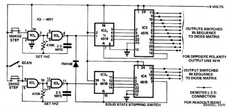
This circuit was designed to make switching of a 48-channel mobile transceiver safe to operate while mobile. The oscillators allow for single-stepping or a scanning function.The scan facility allows for stepping through all 48 channels to check for occupancy or otherwise, and each output is indicated with an LED and labeled accordingly, so at-aglance indication is possible. With full scope of this circuit it is possible to scan 256 channels and by adding more 4 to 16 line encoders etc. you could switch to any required number. (View)
View full Circuit Diagram | Comments | Reading(1403)
DISCO_STROBE_LIGHT
Published:2009/7/6 20:08:00 Author:May

This circuit uses a voltage doubler CR1 and CR2 to obtain about 280 V dc across C1. C2 and R3 form a voltage divider to obtain a dc voltage to change C3 thru R2. When CR3 fires, a high voltage is generated in T1, firing L1.
(View)
View full Circuit Diagram | Comments | Reading(1270)
SAFETY_FLARE
Published:2009/7/6 20:04:00 Author:May


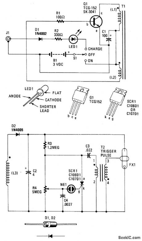
When 51 is on, power is applied to an oscillator composed of Q1, R1, C1, L1, and L2. Coil L1 is the primary winding of T1, and L2 is the feedback winding. When Q1 turns on, its collector current saturates T1's ferrite core. That, in turn, removes the base drive to Q1 through L2. Transistor Q1 then turns off. As the field around L1 and L2 decays, Q1 will eventually turn on again, and the cycle repeats over, and over.Transformer T1 is a step-up, ferritecore, potted-type unit whose secondary;winding (L3) output is rectified by D2 and filtered by C2. That capacitor charges up to around 250 to 300 volts, which is applied to the resistor divider composed of R3 and R4, along with the flash tube FX1.Capacitors C3 and C4 will charge up to around 200 and 100 volts, through R3 and R4, respectively. Flash rate is adjustable via R4. When the charge on C4 gets to around 100 volts, neon lamp NE1 fires discharging C4 into the gate circuit of silicon control rectifier SCR1. The SCR1 turns on discharging C3 into the primary winding of trigger-pulse transformer T2, Transformer T2 is another step-up, pulse-type unit providing an output of around 4 kW across transformer T2's secondary winding.The xenon gas inside FX1 is ionized and a bright flash is emitted. Finally, C3 quickly discharges through L4, and the cycle repeats over, and over.
(View)
View full Circuit Diagram | Comments | Reading(672)
SIMPLE_STROBE
Published:2009/7/6 20:03:00 Author:May

Initially the neon and xenon lamps are not conducting and act like a very high (almost infinite) resistance. Capacitors C1 and C4 in conjunction with D1 and D2 form a voltage doubler circuit, which can charge C2 up to about 300 Vdc after several ac cycles.Voltage increases as current is supplied through R1 and R2. Neon bulb I1 will all of a sudden start to conduct when the voltage across C3 reaches 11's ionization potential.While conducting, the resistance of the bulb will be relative low. Due to this sudden conduction, a pulse of current will pass through the primary of T1. The turns ratio is such that about 400 V will be developed at the secondary. The xenon tube is similar to the neon bulb in that it produces light when the gas ionizes and conducts. However, it is designed so that an external signal (the 4 kV on the metal ring around the tube) ionizes the gas and initiates the conduction. When F1 conducts, it discharges C2. At this point, the whole cycle starts over again. The purpose of R2 is to vary the rate at which C3 charges, and hence the repetition rate of the strobe. (View)
View full Circuit Diagram | Comments | Reading(981)
STEREO_BALANCE_METER
Published:2009/7/6 20:01:00 Author:May

To use the indicator, switch the amplifier to mono mode and adjust the balance control until both LEDs are equally illuminated. The amplifier is now in perfect stereo mode balance. (View)
View full Circuit Diagram | Comments | Reading(0)
STEREO_BALANCE_TESTER
Published:2009/7/6 20:00:00 Author:May

The meter will show volume and tone control balance between left and right stereo amplifiers. For maximum convenience the meter is a zero-center type. Resistors are five percent or better and the diodes a matched pair. Optimum stereo level and phase balance occurs for matched speakers when the meter indicates zero. If the meter indicates either side of zero, the levels are not matched or the wires are incorrectly phased. Check phasing by making certain the meter leads are connected to the amplifier hot terminals and the common leads go to ground. (View)
View full Circuit Diagram | Comments | Reading(846)
STAIRCASE_GENERATOR_Ⅱ
Published:2009/7/6 19:59:00 Author:May

View full Circuit Diagram | Comments | Reading(504)
STAIRCASE_GENERATOR
Published:2009/7/6 19:57:00 Author:May

The circuit uses three BiMOS op amps. Two CA3130's are used, one as a multivibrator and the other as a hysteresis switch. The third amplifier, a CA3160, is used as a linear staircase generator. (View)
View full Circuit Diagram | Comments | Reading(3856)
THREE_PHASE_SQUARE_WAVE_OUTPUT_GENERATOR
Published:2009/7/6 19:56:00 Author:May
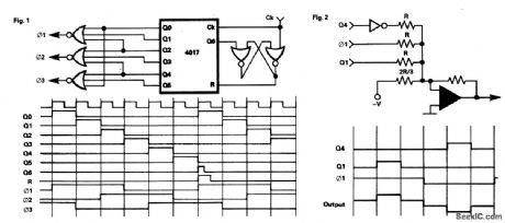
This circuit gives a 3 phase square-wave output for a variable speed motor drive.Operation is straightforward, the 4017 counter is synchronously reset after six clock inputs. The six outputs are combined to give the required waveforms. It is interesting to note that although NOR gates are shown, OR gates will give effectively the same result. The circuit can be extended as shown in Fig. 2 to give pseudo-sine waves if that is required, but that will diminish the simplicity of the circuit.
(View)
View full Circuit Diagram | Comments | Reading(1242)
LINE_FREQUENCY_SQUARE_WAVE_GENERATOR
Published:2009/7/6 19:55:00 Author:May

With only three components and a buffer, a line frequency square wave having a 1:1 duty cycle may be derived from the power supply. During the alternate half-cycle, however, A is effectively clamped to -0.7 V by Dl in the bridge which offsets the forward voltage across D2 giving an input to IC1 of approximately 0 V. When A rises above + 5 V, D2 is reverse biased and remains at +5 V. R1 is needed to load the transformer secondary maintaining a distortion-free waveform at A during the time the diode bridge is not conducting. C1 although not essential may be required to remove transients.
(View)
View full Circuit Diagram | Comments | Reading(726)
FREQUENCY_DOUBLER
Published:2009/7/6 9:38:00 Author:May
The output contains the sum component, which is twice the frequency of the input, since both input signals are the same frequency. (View)
View full Circuit Diagram | Comments | Reading(0)
PULSE_WIDTH_MULTIPLIER
Published:2009/7/6 9:37:00 Author:May
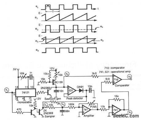
This circuit for multiplying the width of incoming pulses by a factor greater or less than unity is simple to build and has the feature that the multiplying factor can be selected by adjusting one potentiometer only. The multiplying factor is determined by setting the potentiometer in the feedback of the 741 amplifier. The input pulses e1, width T and repetition period T is used to trigger a sawtooth generator at its rising edges to produce the waveform e2 having a peak value of E volts. This peak value is then sampled by the input pulses to generate the pulse train e3 having an average value of e4(= ET/T) which is proportional to T and independent on T. The dc voltage e4 is amplified by a factork and compared with sawtooth waveform e2 giving output pulses of duration kT. The circuit is capable of operating over the frequency range 10 kHz- 100 kHz. Note that ic should be chosen less than T/T to ensure accurate pulse-width multiplication. (View)
View full Circuit Diagram | Comments | Reading(1012)
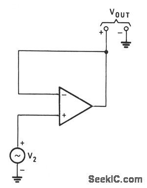
VOLTAGE_FOLLOWER
Published:2009/7/6 9:33:00 Author:May
View full Circuit Diagram | Comments | Reading(0)
Phase_control_circuit_that_uses_a_PUT
Published:2009/7/22 4:11:00 Author:Jessie
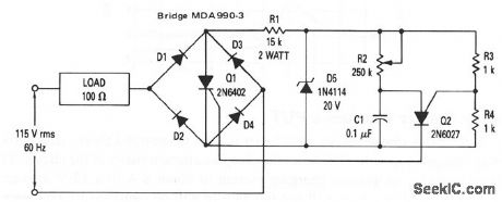
This circuit shows a PUT that is used to control phase of an SCR. The relaxation oscillator that is formed by Q2 provides conduction control of Q1 from 1 to 7.8 ms (21.6° to 168.5°). This constitutes control of over 97% of the power that is available to the load. Only one SCR is needed to provide phase control of both the positive and negative portion of the sine wave, by putting the SCR across the bridge, which is composed of diodes D1 through D4. (View)
View full Circuit Diagram | Comments | Reading(642)
SIMPLE_FOLLOWER
Published:2009/7/6 9:33:00 Author:May
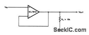
View full Circuit Diagram | Comments | Reading(461)
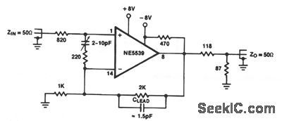
HIGH_FREQUENCY_NONINVERTING_FOLLOWER
Published:2009/7/6 9:33:00 Author:May
View full Circuit Diagram | Comments | Reading(523)
Long_duration_timer_that_uses_a_PUT
Published:2009/7/22 4:08:00 Author:Jessie
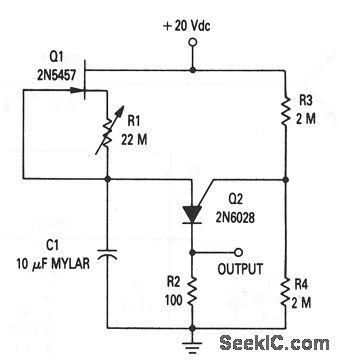
This circuit shows a PUT that is used as a long-duration (up to about 20 minutes) timer. The circuit is similar to that of Fig. 9-20. However, the PUT is superior to the UJT in long-duration timers because the PUT has a lower peak-point firing current (making it possible to charge the capacitor over a longer time). (View)
View full Circuit Diagram | Comments | Reading(649)
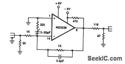
HIGH_FREQUENCY_INVERTING_FOLLOWER
Published:2009/7/6 9:32:00 Author:May
View full Circuit Diagram | Comments | Reading(651)
LIQUID_LEVEL_MONITOR
Published:2009/7/6 9:31:00 Author:May

This monitor uses a common 741 amp conft-gured as a comparator and a low cost nontransistor as an output driver. With no liquid detected, a volt-age of about 2.92 V is present in the op amp's inverting input at pin 2. The 100-KΩ resistors establish a reference voltage of +2.5 V at the non-inverting input at pin 3 of the op amp. Under those conditions, the op amp's output is -3.56 V, which keeps the 2N2222 transistor turned off and the voltage across its 1-KΩ output load resistor at 0 V. When liquid reaches the probes, the 3.3-MΩ and 22-KΩ resistor circuit conductively connects to ground. When enough current, about 1.4 μA, flows through the liquid, the small 30 mV drop developed across the 22-KΩ resistor drives the op amp to deliver an output voltage of about 4.42 V. This volt-age then drives a 2N2222 transistor into saturation, which generates a voltage drop of about 3.86 V across its 1-KΩ output load resistor. (View)
View full Circuit Diagram | Comments | Reading(937)
Discrete_component_audio_amplifier_7_to_35_W
Published:2009/7/22 4:07:00 Author:Jessie


This circuit provides a 7- to 35-W output, depending on power source and component values (as shown), with overload protection. Figures 1-18B and 1-18C show the PC-board layout and performance characteristics, respectively. (View)
View full Circuit Diagram | Comments | Reading(1041)
| Pages:1027/2234 At 2010211022102310241025102610271028102910301031103210331034103510361037103810391040Under 20 |
Circuit Categories
power supply circuit
Amplifier Circuit
Basic Circuit
LED and Light Circuit
Sensor Circuit
Signal Processing
Electrical Equipment Circuit
Control Circuit
Remote Control Circuit
A/D-D/A Converter Circuit
Audio Circuit
Measuring and Test Circuit
Communication Circuit
Computer-Related Circuit
555 Circuit
Automotive Circuit
Repairing Circuit