
Circuit Diagram
Index 1029
PORTABLE_RF_BURST_GENERATOR
Published:2009/7/6 9:04:00 Author:May

The circuit generates low-level rf bursts having frequencies as high as 10 MHz, thus permitting field testing of high frequency receivers. A jumper-selectable binary fraction (1/2 to 1/256 of the Y1 crystal frequency gates the output rf signal. Output amplitude (open circuit) is approximately 100 mV; output impedance is approximately 49Ω. The rf source is a clock oscillator based on a 3.58-MHz, color-burst crystal and two inverting buffers. The oscillator drives two cascaded 4-bit binary counters, IC2, and the sync signal resets the counters with a logic-high pulse-logic low at the counters. Select the desired output frequency by adding a jumper to one of the counter's eight output lines, which provides an enable signal for the two 3-state output buffers. The square-wave output at IC1, pin 11, is attenuated by R1, R2, and R3 to fix the output resistance at approximately 49Ω. Resistor R3 is the only critical component; for clean gating, isolate it from the rest of the circuit. (View)
View full Circuit Diagram | Comments | Reading(1213)
TRANSISTOR_FLASHER
Published:2009/7/6 9:04:00 Author:May

This astable multivibrator uses incandescentlamps In place of collector load resistors. The lamps flash on and off alternately. (View)
View full Circuit Diagram | Comments | Reading(870)
TWO_STATE_NEON_OSCILLATOR
Published:2009/7/6 9:02:00 Author:May
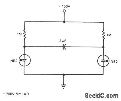
The number of lamps is easily increased in this oscillator. (View)
View full Circuit Diagram | Comments | Reading(588)
ALTERNATING_LED_FLASHER_1
Published:2009/7/6 9:02:00 Author:May

The alternating LED flasher is simply a two-transistor oscillator with LEDs connected to the collector of each transistor, so that they light in time with the circuit's oscillations. (View)
View full Circuit Diagram | Comments | Reading(1729)
60_W_FLASHING_LIGHT
Published:2009/7/6 9:01:00 Author:May

The 2N6101 transistor should be mounted on a small heatsink. The 300-KΩ resistor controls the off period and might need to be adjusted if transistor gains are high. The 100-KΩ resistor controls the on period. (View)
View full Circuit Diagram | Comments | Reading(785)
CMOS_FLASHER
Published:2009/7/6 8:59:00 Author:May
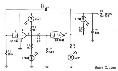
Uses a low cost CMOS IC to turn four LEDs on and off at a rate that is set by the values of R1, R2, C1, and C2. The pulse rate for the component values given for R1 and R2 is about one cycle every four seconds. By lowering the values of R1 and R2 to 220 KΩ, the pulse rate increases to 1 Hz. The LEDs flash in pairs, with LED1 and LED4 tuming together for one half of the time period, while LED2 and LED3 are on for the other half. The on/off duration of each pair of LEDs can be increased or decreased by changing the value of one of coupling capacitors C1 or C2. Increasing either capacitor's value by a factor of 10 will also increase the ON time of a pair of the LEDs for about the same factor. (View)
View full Circuit Diagram | Comments | Reading(573)
ALTERNATING_LED_FLASHER
Published:2009/7/6 8:58:00 Author:May

The timing components are R1, R2, and Ct. C1 is a bypass capacitor used to reduce the effects of noise. At start-up, the voltage across Ct is less than the trigger level voltage (1/3 VDD), causing the timer to be triggered via pin 2. The output of the timer at pin 3 increases, turning LED1 off, LED2 on, the discharge transistor at pin 7 off, and allowing Ct to charge through resistors R1 and R2. When capacitor Ct charges to the upper threshold voltage (2/3 VDD), the flip-flop is reset and the output at pin 3 decreases. LED1 is turned on, LED2 is turned off, and capacitor Ct discharges through resistor R2 and the discharge transistor. When the voltage at pin 2 reaches 1/3 VDD, the lower threshold or trigger level, the timer trig-gers again and the cycle is repeated.The totem-pole output at pin 3 is a square wave with a duty cycle of about 50%. The output alternately turns on each LED at slightly less than one blink per second. If the unit is battery operated, the TLC555 uses minimum current to produce this function. With a 9-V battery, the circuit draws 5 mA (noload) and 15 mA when turning on an LED. Most of the on current is for the LED. (View)
View full Circuit Diagram | Comments | Reading(737)
PT2399 Digital Reverb Processing Integrated Circuit
Published:2011/7/23 4:44:00 Author:Michel | Keyword: Digital Reverb, Integrated Circuit


PT2399 is one typical karaoke echo processing integrated circuit which is widely used in CD, VCD, DVD, TV sound and karaoke.
First,PT2399 Inside Circuit Block Diagram and Pins Functions
There are A/D and D/A converter within PT2399 IC.And the input analog voice signal needs digital processing.Its inside circuit block diagram of the intergrated block is shown s picture 1.And the pins functions of the IC is shown as table 1.
Table 1:Pins Functions of PT2399 IC
Second,PT2399 Typical Application Circuit
According to PT2399 internal and external resistance connection,its typical equivalent circuit is shown as picture 2.
(View)
View full Circuit Diagram | Comments | Reading(9209)
FIVE_LAMP_NEON_FLASHER
Published:2009/7/6 8:52:00 Author:May
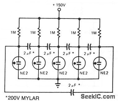
In this circuit, the number of lamps can be increased almost without limit. (View)
View full Circuit Diagram | Comments | Reading(476)
STRAIN_GAUGE_SIGNAL_CONDITIONER_WITH_BRIDGE_EXCITATION
Published:2009/7/6 8:51:00 Author:May
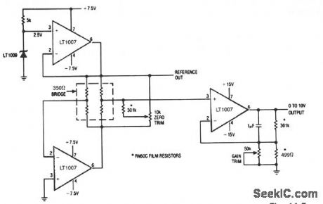
The LT1007 is capable of providing excitation current directly to bias the 350-Ω bridge at 5 V. With only 5 V across the bridge, as opposed to the usual 10 V, total power dissipation and bridge warm-up drift is reduced. The bridge output signal is halved, but the LT1007 can amplify the reduced signal accurately. (View)
View full Circuit Diagram | Comments | Reading(594)
INCANDESCENT_LIGHT_FLASHER
Published:2009/7/6 8:50:00 Author:May

View full Circuit Diagram | Comments | Reading(916)
BRIDGE_TRANSDUCER_AMPLIFIER
Published:2009/7/6 8:50:00 Author:May
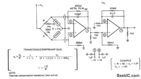
In applications involving strain gauges, accelerometers, and thermal sensors, a bridge transducer is often used. Frequently, the sensor elements are high resistance units requiring equally high bridge resistance for good sensitivity. This type of circuit then demands an amplifier with high input impedance, low bias current and low drift. The circuit shown represents a possible solution to these general requirements. (View)
View full Circuit Diagram | Comments | Reading(0)
REMOTE_SENSOR_LOOP_TRANSMITTER
Published:2009/7/6 8:49:00 Author:May
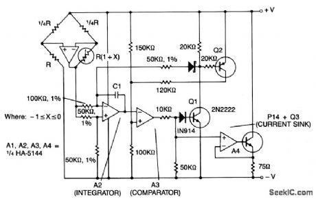
This circuit shows amplifier A1 as a sensor amplifier in a bridge configuration. Amplifiers A2 and A3 are configured as a voltage to frequency converter and A4 is used as the transmitter. This entire sensor/ transmitter can be powered directly from a 4 to 20 mA current loop.
The bridge configuration produces a linear output with respect to the changes in resistance of the sensor. The voltage at the output of Al causes the integrator output A2 to ramp down until it crosses the comparator threshold voltage of A3. A3 turns on Q1 and Q2. A1 causes the output of A2 to ramp up at a rate nearly equal to its negative slope, while Q2 provides hysteresis for the comparator. In addition, Q1 and Q2 help eliminate changes in power supply loop voltage. Amplifier A4 and Q3 are configured as a constant current sink which turns on when the comparator current increases. The resulting increase in loop current transmits the frequency of the V/F converter back to the control circuitry.
(View)
View full Circuit Diagram | Comments | Reading(902)
SCR_FLASHER
Published:2009/7/6 8:48:00 Author:May
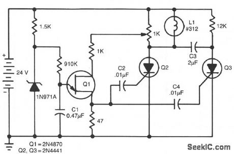
This dc flasher uses two SCRs and a unijunction oscillator clock to set the flash rate, which canbevaried by changing the value of C1. (View)
View full Circuit Diagram | Comments | Reading(787)
SCR_OHASER
Published:2009/7/6 8:47:00 Author:May
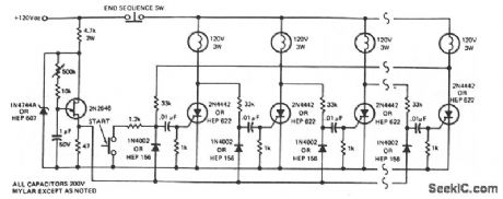
Each lamp lights in succession to give the appearance of a growing column. (View)
View full Circuit Diagram | Comments | Reading(481)
ACCURATE_NULL_VARIABLE_GAIN_CIRCUIT
Published:2009/7/6 8:46:00 Author:May
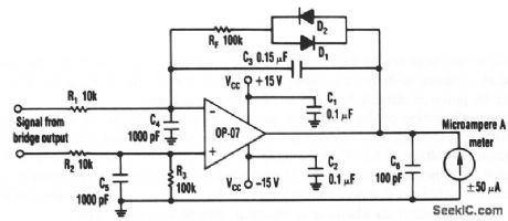
The circuit can use any general-purpose,low-offset,low-drift op amp,such as the OP-07.The differential signal from the bridge feeds an amplifier that drives an ordinary,rugged±50-μA meter. Near the null point,however, the drastically reduced signal level from the bridge requires very high gain to achieve a high null resolutio.To provide the variable-gain feature,the op amp's feedback path needs a dynamic resistance that increases as the input signal drops,Two common signal diodes,Dl and D2,in an antiparallel configuration in the feedback path supply function for all positive and negative inputs.To stabilize the opamp circuit at high gain,capacitors C3,C5,and C6 reduce response to high frequencies ;capacitors C1 andC2 bypass the amplifier's power supplies. (View)
View full Circuit Diagram | Comments | Reading(600)
9_digit_universal_counter_using_the_ICM7226A_40_pin_DIP
Published:2009/7/22 5:29:00 Author:Jessie
9-digit universal counter using the ICM7226A 40-pin DIP (courtesy Intersil, Inc.). (View)
View full Circuit Diagram | Comments | Reading(1391)
Hi_fi_tone_control_with_high_impedance_input
Published:2009/7/22 5:27:00 Author:Jessie
The JFET provides both high input impedance and low noise to buffer an op-amp feedback-type tone control. (View)
View full Circuit Diagram | Comments | Reading(1464)
Amplifier_for_piezoelectric_transducers
Published:2009/7/22 4:32:00 Author:Jessie

This circuit shows an LM108 amplifier for high-impedance ac transducers, such as a piezoelectric accelerometer. The circuit has input resistance that is much greater than the dc return resistor values. This is accomplished by bootstrapping the resistors to the output. With such an arrangement, the lower cutoff frequency of a capacitive transducer is determined more by the RC output of R1 and C1 than by resistor values and the equivalent capacitance of the transducer. (View)
View full Circuit Diagram | Comments | Reading(3271)
SINGLE_LAMP_FLASHER
Published:2009/7/6 8:45:00 Author:May

The flash rate is controlled by a complementary multivibrator consisting of an npn and a pnptransistor. (View)
View full Circuit Diagram | Comments | Reading(799)
| Pages:1029/2234 At 2010211022102310241025102610271028102910301031103210331034103510361037103810391040Under 20 |
Circuit Categories
power supply circuit
Amplifier Circuit
Basic Circuit
LED and Light Circuit
Sensor Circuit
Signal Processing
Electrical Equipment Circuit
Control Circuit
Remote Control Circuit
A/D-D/A Converter Circuit
Audio Circuit
Measuring and Test Circuit
Communication Circuit
Computer-Related Circuit
555 Circuit
Automotive Circuit
Repairing Circuit