
Circuit Diagram
Index 1025
A_D_converter_for_nonratiometric_transducer_inputs
Published:2009/7/23 0:56:00 Author:Jessie
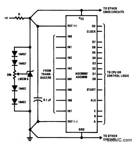
This circuit converts the output from 8 nonratiometric or absolute transducers to an 8-bit digital word using an ADC0808/0809, under control of a CPU or similar digital logic. The timing and internal functions shown in Fig. 6-13B and 6-13C also apply to this circuit. The LM336-5 acts as both a regulator and reference (for a 5-V or larger supply). Dropping resistor R is chosen so that, for the whole range of supply currents needed by the system (not just the ADC), the LM336-5 will stay in regulation. Again, use separate supply and reference traces to minimize noise. (View)
View full Circuit Diagram | Comments | Reading(478)
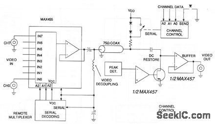
Video_system_remote_multiplexer_box
Published:2009/7/22 22:37:00 Author:Jessie

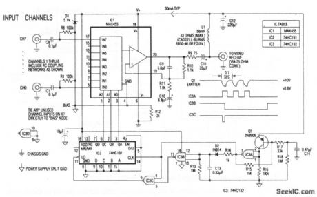
The heart of the remote multiplexer box in the single-coax video system (Fig. 3-14) is a combination 8-channel multiplexer and amplifier (IC1). C11couples the MUX baseband video output to the coax, and L1 decouples the video from dc power arriving on the same line. This power (about 30 mA at 10 V) supplies all circuitry in the multiplexer box. Channel-select signals generated at the interface box (11 pulse for channel 0, 8 pulses for channel7) pulse the 10-V supply to 8.8 V and back at a 10-Hz rate. Q1 and associated components in the remote multiplexor box convert these pulses to 5-V logic levels, which block the 4-bit counter IC2. In turn, IC2 selects the desired multiplexor channel. The first pulse of a burst selects channel 0. Subsequent pulses, arriving before the discharge of timeout network R13/C 13 advance IC2 by one count each. Thus, channel 0 appears almost instantly, and channel 1, when selected, appears near the end of a 0.8-s burst. (View)
View full Circuit Diagram | Comments | Reading(2985)
TELEPHONE_HOLD_BUTTON
Published:2009/7/6 20:39:00 Author:May


The on-hook (no load) voltage across the red-green wires will be 48 V or slightly less when all telephones are on-hook (disconnected). When any telephone goes off-hook the load current flowing in the telephone causes the voltage to fall below 5 volts dc.Although the telephone hold is connected across the red-green wires, silico1i control rectifier SCR1 is open; so there is no current path across the telephone line. To hold the call, depress normally-open switch S1 and hang up the telephone (still depressing S1). When the phone goes on-hook the red-green voltage jumps to 48 volts dc. Since switch S1 is closed, a positive voltage is applied to SCR1's gate, which causes SCR1 to conduct, thereby completing the circuit across the telephone line through D1, LED1, R1, and SCR1. The current that flows through those components also causes the LED to light up-indicating that the telephone line is being held. The effective load across the red-green wires is the 1500 ohm value of R1, which is sufflcient to seize the line while limiting the current through the LED to a safe value. When the telephone, or an extension, is once again placed off-hook the red-green voltage falls to 5 volts or less.But diode D1 has a normal voltage drop-called the breakover voltage-of 0.7 volts, and the LED has a forward drop of 2.0 volts. Excluding the voltage drop across R1 there is a maximum of 2.3 volts available for SCR1, which is too low to maintain conduction; so SCR1 automatically opens the hold circuit when any telephone goes off-hook. (View)
View full Circuit Diagram | Comments | Reading(95)
Op_amp_circuits_titles_and_descriptions
Published:2009/7/22 22:36:00 Author:Jessie
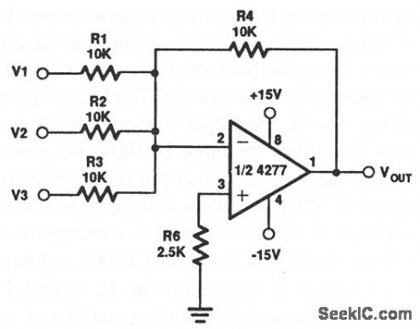
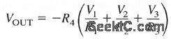
Because R1 through R4 are all the same value, VOUT=V1+V2+V3. Notice that R6 equals the parallel resistance of R1 through R4 and VOUT= -R4. (View)
View full Circuit Diagram | Comments | Reading(621)
CMOS_A_D_converter_with_complementary_logic_0_V_to__VSUBREF_SUB_input
Published:2009/7/22 22:34:00 Author:Jessie
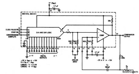
The ADC used in this circuit combines the SAR, the DAC and the comparator in a single IC. Compare this to the A/D of Fig. 6-43. (View)
View full Circuit Diagram | Comments | Reading(509)
FSK_SQUARE_TRIANGLE_GENERATOR_
Published:2009/7/6 20:39:00 Author:May

Uses Exar XR-2207 FSK modulator connected for single-supply operation, to produce triangle or square FSK outputs for either single-channel or two-channel multiplex operation. Used in transmitting digital data over telecommunication links. Table gives equations for selecting timing resistors R1-R4; resistor values are in ohms, C0is in farads, and frequency is in hertz. For optimum stability, R1 and R3 should be in range of 10K to 100K. For two-channel multiplex, make connections shown by dotted lines.- Phase-Locked Loop Data Book, Exar Integrated Systems, Sunnyvale, CA, 1978, p 57-61. (View)
View full Circuit Diagram | Comments | Reading(1264)
Video_power_and_channel_select_on_a_single_coax
Published:2009/7/22 22:34:00 Author:Jessie

In this video system, a single coaxial cable carries power to the remote location, selects one of eight video channels, and returns the selected signal. The system can choose one of several remote surveillance-camera signals, for example, and display the picture on a monitor near the channel-select box. Circuit details are shown in Figs. 3-15 and 3-16. (View)
View full Circuit Diagram | Comments | Reading(577)
PLUG_IN_REMOTE_TELEPHONE_RINGER
Published:2009/7/6 20:37:00 Author:May

This device consists of a ring detector connected to the telephone line. When the telephone rings, the ring detector impresses high-frequency pulses on the ac power line.A receiver placed anywhere on the same power line detects these pulses and emits an audible tone in synchronization with the telephone signal. (View)
View full Circuit Diagram | Comments | Reading(1033)
Stabilized_wideband_cable_driving_amplifier_with_low_input_capacitance
Published:2009/7/22 22:32:00 Author:Jessie
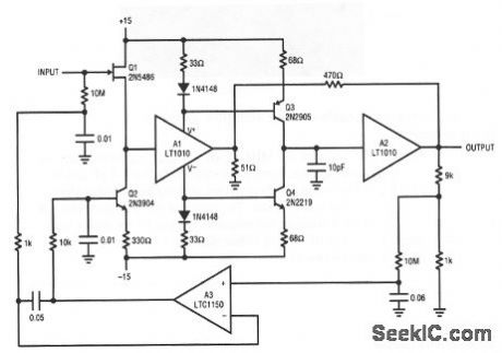
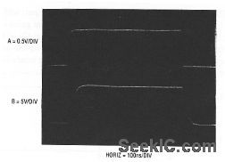
This circuit has over 20 MHz of small-signal bandwidth driving 100-mA loads, capacitance or cable. Input capacitance is below 1.5 pF and bias current is about 100 pA. The output is fully protected, making the amplifier ideal as a video A/D input buffer or as a cable driver. The amplifier also permits wideband probing when scope probe loading is not tolerable. Figure 3-13B shows large-signal performance at a gain of 10, driving 10 feet of cable. A fast input pulse (trace A) produces the output shown (trace B). (View)
View full Circuit Diagram | Comments | Reading(657)
REMOTE_TELEPHONE_MONITOR
Published:2009/7/6 20:35:00 Author:May

This device monitors sounds in home or office when a telephone is called from a remote location. (View)
View full Circuit Diagram | Comments | Reading(667)
CAPACITANCE_METER
Published:2009/7/6 20:33:00 Author:May

U1a is an oscillator and U1b the measurement part of the circuit. It converts unknown capacity into a pulse-width modulated signal the same way an automotive dwell meter works. The meter is linear so the fraction or percentage of time that the output is high is directly proportional to the unknown capacitance (CX in the schematic). Meter M1 reads the average voltage of those pulses since its mechanical frequency response is low compared to the oscillator frequency of U1a. (View)
View full Circuit Diagram | Comments | Reading(2)
Audio_mlxer
Published:2009/7/22 22:08:00 Author:Jessie

In many audio applications,it is desirable to provide a mixer tocombine or select several inputs,Such applications include public-address systems,where more than one microphone is used,tape recorders,hi-fi phonographs,guitar amplifiers,etc.This circuit provides for mlxlng of 600-Ω dynamic microphones, each with an output level of 10 mV The circuit operates from a 24-V Supply and delivers 5-V output,with a dynamic range of 80 dB. (View)
View full Circuit Diagram | Comments | Reading(1725)
HIGH_ISOLATION_TELEPHONE_RINGER
Published:2009/7/6 20:33:00 Author:May

The diode rectifies the ringing signal to supply the operating power to the audio relaxation oscillator made up of L1, L2, R1, R2, and C. Moreover, L2 together with Q1 acts as an opto-isolator, totally isolating the telephone line from the rest of the circuit.The oscillator audio frequency is optically coupled to the photo-Darlington which drives Q2 and thus the speaker. The 10 μF capacitor is not large enough to smooth the ringing ripple completely. This results in frequency modulation of the audio oscillator giving it an attention-getting warble.
(View)
View full Circuit Diagram | Comments | Reading(661)
DIGITIZING_POT_POSITION
Published:2009/7/6 20:32:00 Author:May
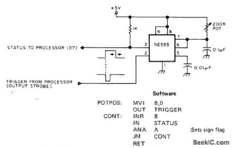
Converts position of pot arm into digital value, using NE555 timer and several bytes of program in 8008 or 8080 microprocessor having 2.5-μs clock. NE555 is triggered at pin 2 by 0UT TRIGGER instruction. Program monitors output at pin 3 in loop that increments B register. When NE555 times out, program exits from subroutine and B register contains digital representation of pot position.-J. M. Schulein, Pot Position Digitizing Idea, BYTE, March 1976, p 79. (View)
View full Circuit Diagram | Comments | Reading(1026)
Optically_coupled_Schmitt_trigger
Published:2009/7/22 22:07:00 Author:Jessie
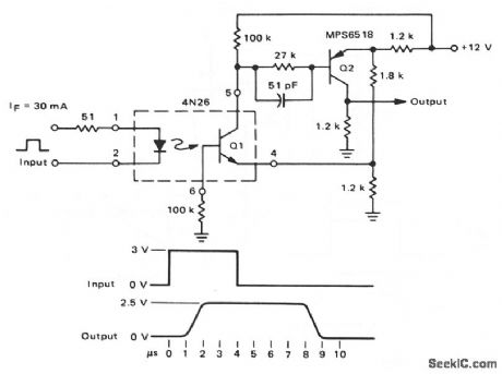
This circuit uses the 4N26 transistor as part of a Schmitt trigger. When Q1 conducts in response to an input pulse, Q2 conducts and the output is high.When the input pulse is removed from the 4N26, Q1 shuts off, and the output is low. With the values shown, the tum-off delay is about 2 μs, and the turn-off delay is about 6 ps. Speed can be improved by lowering the value of the Q1 base resistance from 100 kΩ, but the drive requirements must be increased. (View)
View full Circuit Diagram | Comments | Reading(1998)
PHONE_LIGHT
Published:2009/7/6 20:32:00 Author:May

When the phone does ring the triac is triggered into conduction by a signal applied to its gate (G) through a bilateral switch (diac), D2. The triac acts as a switch, conducting only when a signal is present at the gate.
(View)
View full Circuit Diagram | Comments | Reading(778)
Optocoupler_that_is_used_as_a_pulse_stretcher
Published:2009/7/22 22:03:00 Author:Jessie
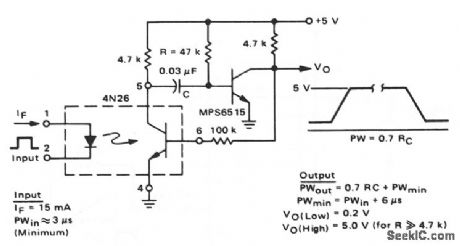
This circuit shows a 4N26 combined with a standard one-shot to form a pulse stretcher. A pulse of about 3 μs at 15 mA triggers the circuit. The output pulse amplitude is a function of supply voltage on the output side, and is independent of the input. (View)
View full Circuit Diagram | Comments | Reading(616)
Diode_diode_coupler
Published:2009/7/22 22:00:00 Author:Jessie

This circuit shows a 4N26 that is used as a diode/diode coupler. The 4N26 emitter is left open, the load resistor is connected between base and ground, and the collector is tied to the supply. Using the 4N26 in this way reduces the switching time from about 2 or 3 μs to 100 ns. (View)
View full Circuit Diagram | Comments | Reading(3635)
CIRCUIT_MONITORS_BLINKING_PHONE_LIGHTS
Published:2009/7/6 20:31:00 Author:May

A 2N5777 photo-Darlington cell picks up blinking light from the transparent plastic buttons. The power is switched ON and OFF by a hibeta 2N3904 transistor. The circuit's 9 V battery can be left continuously connected. Less than a microampere is drawneven with normal, office ambient light and the phone lights not flashing. For noisy locations, the tone can be made louder with an output transformer (ratio of 250:8) or a 100 ohm speaker that replaces the 22 ohm resistor in the output. (View)
View full Circuit Diagram | Comments | Reading(1613)
31_2_DIGIT_A_D_CAPACITANCE_METER
Published:2009/7/6 20:30:00 Author:May

The circuit charges and discharges a capacitor at a crystal-controlled rate, and stores on a sample-and-difference amplifier the change in voltage achieved. The current that flows during the discharge cycle is averaged, and ratiometrically measured in the a/d using the voltage change as a reference. Range switching is done by changing the cycle rate and current metering resistor. The cycle rate is synchronized with the conversion rate of the a/d by using the externally divided internal oscillator and the internally divided back plane signals. For convenience in timing, the switching cycle takes 5 counter states, although only four switch configurations are used. Capacitances up to 200 μF can be measured, and the resolution on the lowest range is down to 0.1 pF.
The zero integrator time can be set initially at 1/3 to 1/2, the minimum auto-zero time, but if an optimum adjustment is required, look at the comparator output with a scope under worst-case overload conditions. The output of the delay timer should stay low until after the comparator has come off the rail, and is in the linear region (usually fairly noisy).
(View)
View full Circuit Diagram | Comments | Reading(858)
| Pages:1025/2234 At 2010211022102310241025102610271028102910301031103210331034103510361037103810391040Under 20 |
Circuit Categories
power supply circuit
Amplifier Circuit
Basic Circuit
LED and Light Circuit
Sensor Circuit
Signal Processing
Electrical Equipment Circuit
Control Circuit
Remote Control Circuit
A/D-D/A Converter Circuit
Audio Circuit
Measuring and Test Circuit
Communication Circuit
Computer-Related Circuit
555 Circuit
Automotive Circuit
Repairing Circuit