
Circuit Diagram
Index 1028
LIQUID_LEVEL_CHECKER
Published:2009/7/6 9:29:00 Author:May
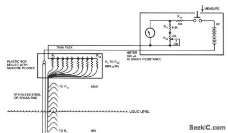
Although many circuits use the varying-capacitance method for checking liquid levels, this simple resistive circuit is much easier to construct. Even a tank of a liquid, such as water, has sufficient conduc-tive salts in solution for this method to work. The probe uses a metal rod that supports 10 insulated wires, which have stripped ends pointing down. As the level of liquid rises, resistors R1 through R10 are succes-sively brought into circuit, each drawing an extra 10 μA through the meter. Shunt resistors R11 and R13 calibrate the meter for a full-scale reading when the tank is full. Resistor R12 limits the current through the meter. If tank isn't rectangular-ie, if the volume of the liquid it contains isn't directly proportional to the liquid's depth-space the resistors accordingly or use a nonlinear progression of resistor values and retain constant resistor spacing. (View)
View full Circuit Diagram | Comments | Reading(581)
Discrete_component_audio_amplifier_3_to_5_W_npn_driver
Published:2009/7/22 4:05:00 Author:Jessie
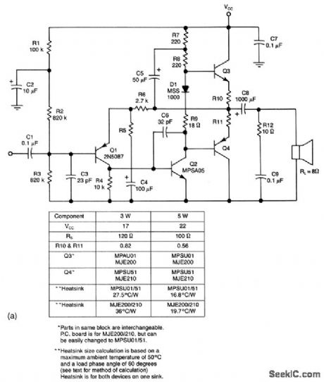

This circuit provides a 3- or 5-W output, depending on power source and component values, with an npn driver, and overload protection. Figures 1-17B and 1-17C show the PC-board layout and performance characteristics, respectiVely.
(View)
View full Circuit Diagram | Comments | Reading(921)
Low_frequency_divider
Published:2009/7/22 4:05:00 Author:Jessie
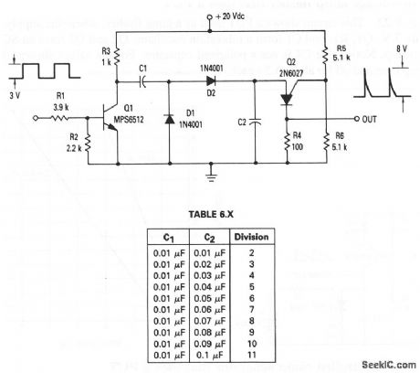
This circuit shows a PUT that is used as a frequency divider, where the ratio of C1 and C2 determines the amount of division. For a 10-kHz input frequency, and an amplitude of 3 V, Table 6-X shows the values for C1 and C2 that are needed to divide by values from 2 to 11. The division range can be changed by changing the ratio R6/(R6 + R5). With a given C1 and C2, increasing the resistance ratio increases the division range. (View)
View full Circuit Diagram | Comments | Reading(0)
Discrete_component_audio_amplifier_3_to_5_W
Published:2009/7/22 4:03:00 Author:Jessie

This circuit provides a 3- or 5-W output, depending on power source and component values, with a pnp driver and overload protection. Figures 1-16B and 1-16C show the PC-board layout and performance characteristics, respectively. (View)
View full Circuit Diagram | Comments | Reading(693)
SOIL_MOISTURE_METER
Published:2009/7/6 9:26:00 Author:May

IC1, an Intersil ICL7106, contains an a/d converter, a 3 1/2-digit LCD driver, a clock, a voltage refer-ence, seven segment decoders, and display drivers. A similar part, the ICL7107, can be used to drive seven segment LEDs. The probe body is a five-inch length of light-weight aluminum tubing. The leads from the circuit are connected to the body and tip of the probe. The sensor functions as a variable resistor that varies Q1's base current, hence its collector current. The varying collector current produces a varying voltage across 100 Ω resistor R7, and that voltage is what IC1 converts for display.The LCD consumes about 25 μA, and IC1 consumes under 2 mA, so the circuit will run for a long time when it is powered by a standard 9-V battery. Current drain of the two 1.5-V AA cells is also very low: under 300 μA.To calibrate, rotate R3 to the center of its range. Then place the end of the probe into a glass of water and adjust R8 for a reading of 100. When you remove the probe from the water, the LCD should indicate 000. You might have to adjust R3 slightly for the display to indicate 000. If so, readjust R8 with the probe immersed. Check for a reading of 000 again with probe out of water. (View)
View full Circuit Diagram | Comments | Reading(3543)
Voltage_controlled_ramp_generator_that_uses_a_PUT
Published:2009/7/22 4:01:00 Author:Jessie
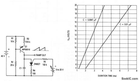
This circuit shows a PUT used as a VCRG. Figure 9-23B shows a plot of voltage-ver sus-ramp duration for two values of C1. (View)
View full Circuit Diagram | Comments | Reading(625)
PCF8598 I2C Bus Control and Storage Integrated Circuit
Published:2011/7/29 0:13:00 Author:Michel | Keyword: Bus Control, Storage, Integrated Circuit

PCF8598 is I2C bus control and storage integrated circuit and it is widely used in KonKa WM series color TVs.
First,Functions Features
PCF8598 integrated circuit contains the I2C bus circuit, program control circuit, memory storage data circuit, the memory address processing circuit and some other auxiliary functions circuit.
Second,Pins Functions and Data
PCF8598 IC adopts 8 feet DIP package and its pins and functions on KonKa T2168K color TV are shown as table 1.
Table 1:PCF8598 IC Pins Functions and Data on KonKa T2168K Series Color TVs (View)
View full Circuit Diagram | Comments | Reading(618)
DUAL_LIQUID_LEVEL_DETECTOR
Published:2009/7/6 9:23:00 Author:May

Uses CA3410 quad BiMOS op amp to sense small currents. Because the op amp's input current is low, a current of only 1 μA passing through the sensor will change the converter's output by as much as 10 to 12 V. (View)
View full Circuit Diagram | Comments | Reading(765)
Audio_amplifiers_with_short_circuit_protection
Published:2009/7/22 4:01:00 Author:Jessie


This circuit makes optimum use of economy transistors in discrete-component amplifiers that will operate safely under any usable load conditions, including shorts. Figures 1-15B, 1-15C, and 1-15D show the transistor complement, resistor values/power-supply voltages, and heatsink requirements, respectively, for various power outputs from 35 to 100 W. Input sensitivity is 1 Vrms into 10 kΩ for full-rated output power. Frequency response is less than 3-dB rolloff from 10 Hz to 100 kHz, referenced to t kHz. Power bandwidth is the full-rated output power ±2 dB from 20 Hz to 20 kHz. Figures 1- 15E and 1- 15F show the load sensitivity and power bandwidth. Total harmonic distortion (THD) is less than 0.2% at any power level between 100 mW and full-rated output and at any frequency between 20 Hz and 20 kHz. Inter modulation distortion is less than 0.2% at any power level from 100 mW to the full-rated output (60 Hz and 7 kHz mixed 4 to 1 )
(View)
View full Circuit Diagram | Comments | Reading(1370)
WATER_LEVEL_SENSOR_AND_CONTROL
Published:2009/7/6 9:20:00 Author:May
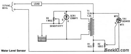
When the water level is low, the probe is out of the water and SCR1 is triggered on. It conducts and imposes a heavy load on transformer T1's secondary winding. That load is reflected back into the primary, gating triac TR1 on, which energizes the load. If the load is an electric valve in the water-supply line, it will open and remain open until the water rises and touches the probe; this shorts SCR1's gate and cathode, thereby turning off the SCR1, which effectively open-circuits the secondary. That open-circuit condition, when reflected back to the primary winding, removes the triac's trigger signal, thereby turning the water off. (View)
View full Circuit Diagram | Comments | Reading(807)
40_TO_43_MHz_VFO_CIRCUIT
Published:2009/7/22 3:59:00 Author:Jessie
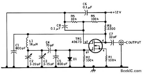
This is a recent 4.0- to 4.3-MHz oscillator design by KGBSU. It seems likely that performance could be improved by increasing the value of C2=C3 and decreasing that of L1 to make the device a true Vacker oscillator. The following component information is recommended by KGBSU: C1 and C5, 800-pF polystyrene; C2, air trimmer for setting calibration, C3, air variable for main tuning; C4, 70-pF, NPO ceramic and silver mica to provide required temperature compensation; C7, 33-pF NPO ce-ramic; C6 and C8, 0.1-μF 25-Vmonolithic capacitor; TR1, 40673 or SK3050 dual-gate MOSFET; D1, 1N4153 or 1N914 silicon signal diode; L1, 16-μF, 34 turns #26 enameled on 3/4-in diameter ceramic form (no slug core), winding length 0.6 inch; all resistors 0.25 W, 5 percent. (View)
View full Circuit Diagram | Comments | Reading(809)
FLOOD_ALARM_OR_TEMPERATURE_MONITOR
Published:2009/7/6 9:17:00 Author:May
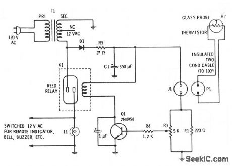
Filtered 15 Vdc is applied to a series circuit consisting of thermistor R2 and parallel combination of resistors R1 and R3. Transistor Q1 acts as a switch whose state is determined by the setting of potentiometer R3, which is first set so just enough current flows into the base to switch on when the thermistor is in contact with air. When the resistance of the thermistor decreases, the voltage at the base of Q1 rises. When the base current reaches the preset level, the transistor conducts and passes current through the reed relay coil, closing the reed relay contacts. Current at the base of transistor Q1 is determined by the environment into which the termistor is inserted. (View)
View full Circuit Diagram | Comments | Reading(643)
Low_voltage_lamp_flasher_that_uses_a_PUT
Published:2009/7/22 3:59:00 Author:Jessie
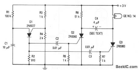
This circuit shows a PUT used as a lamp flasher, where the supply is only 3 V. Q1, R1, and C1 form a relaxation oscillator. Q2 and Q3 form an SCR flip-flop. Notice that C4 is not a polarized capacitor. For the values shown, the lamp is on and off for about 0.5 s each. (View)
View full Circuit Diagram | Comments | Reading(1022)
Long_duration_time_delay
Published:2009/7/22 3:56:00 Author:Jessie
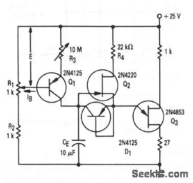
This circuit shows the basic UJT building block (Fig. 9-1), which is used to provide long time delays (up to 10 hours). Q1, R1, R2, and R3 form a constant-current source to charge CE very slowly (a few nA) to provide the long delay. Q2 and D1 (a 2N4125 connected as a diode) provide a separate discharge path to the emitter of UJT Q3. Notice that there is some interaction between R1 and R3 when setting the time delay. (View)
View full Circuit Diagram | Comments | Reading(0)
FLUID_LEVEL_CONTROL
Published:2009/7/6 9:14:00 Author:May
This circuitis designed to detect the presence or absence of aqueous fluids. An ac signal generatedon-chipis passed through two probes within the fluid. A detector determines the presence of the fluid byusmg the probes in a voltage divider circuit and measunng the signal level across the probes. An ac signalis used to prevent plating or dissolving of the probes as Occurs when a dc signal is used. A pinis availablefor connecting an external resistancein cases where the fluid impedanceis not compatible with the internal 13-KΩ divider resistance. (View)
View full Circuit Diagram | Comments | Reading(645)
HIGH_STABILITY_VFO
Published:2009/7/22 3:55:00 Author:Jessie
This circuit was published in the 1960s, but with moderndevices, it is still a useful design approach. The transistors are both 2N384. (View)
View full Circuit Diagram | Comments | Reading(658)
LOW_FLOW_RATE_THERMAL_FLOWMETER
Published:2009/7/6 9:10:00 Author:May
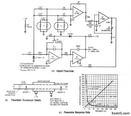
This design measures the differential temperature between two sensors. Sensor T1, located before the heater resistor, assumes the fluid's temperature before it is heated by the resistor. Sensor T2 picks up the temperature rise induced into the fluid by the resistor's heating. The sensor's difference signal appears at A1's output. A2 amplifies this difference with a time constant set by the 10 MΩ adjustment. Fig. 33-1c shows A2's output versus flow rate. The function has an inverse relationship. A3 and A4 linearize this relationship, while simultaneously providing a frequency output. A3 functions as an integrator that is biased from the LT1004 and the 338-KΩ input resistor. Its output is compared to A2's output at A4. Large inputs from A2 force the integrator to run for a long time before A4 can increase, tuming on Q1 and reset-ting A3. For small inputs from A2, A3 does not have to integrate long before resetting action occurs. Thus, the configuration oscillates at a frequency which is inversely proportional to A2's output voltage. Since this voltage is inversely related to flow rate, the oscillation frequency linearly corresponds to flow rate. (View)
View full Circuit Diagram | Comments | Reading(712)
TONE_BURST_GENERATOR_FOR_EUROPEAN_REPEATERS
Published:2009/7/6 9:07:00 Author:May
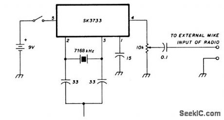
Most European repeaters must be brought up with a 1750-Hz tone. The SK3733 (also known as an ECG1197) IC contains a crystal oscillator and is divided by -256, 1024, 2048, and 4096. A 7168-kHz crystal is used; the divide-by-4096 output produces a 1750-Hz signal. (View)
View full Circuit Diagram | Comments | Reading(812)
LAMP_FLASHER
Published:2009/7/6 9:06:00 Author:May

The circuit is built around two power FETs, which are configured as a simple astable multivibra-tor to alternately switch the two lamps on and off. The rc values given sets the flash rate to about 1/3 Hz. By varying either the resistor or capacitor values, almost any flash rate can be obtained. Increase either C1 and C2, or R1 and R2, and the flash rate slows. Decrease them and the rate increases. (View)
View full Circuit Diagram | Comments | Reading(732)
MINIMUM_COMPONENT_FLASHER
Published:2009/7/6 9:05:00 Author:May
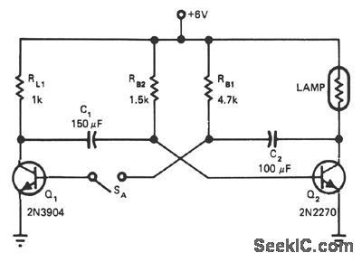
Opening SA, changes the indicator lamp from flashing to steady-lit condition. The 6-V incandes-cent lamp on the collector of Q2 requires about 0.3 A. A 1-KΩ load resistor limits Q1's collector cur-rent to about 6 mA. The circuit is, therefore, asym-metrical with respect to the on currents of the transistors, allowing use of a much smaller transistor for Q1 than for Q2. (View)
View full Circuit Diagram | Comments | Reading(727)
| Pages:1028/2234 At 2010211022102310241025102610271028102910301031103210331034103510361037103810391040Under 20 |
Circuit Categories
power supply circuit
Amplifier Circuit
Basic Circuit
LED and Light Circuit
Sensor Circuit
Signal Processing
Electrical Equipment Circuit
Control Circuit
Remote Control Circuit
A/D-D/A Converter Circuit
Audio Circuit
Measuring and Test Circuit
Communication Circuit
Computer-Related Circuit
555 Circuit
Automotive Circuit
Repairing Circuit