
Circuit Diagram
Index 1035
ASTABLE_MULTIVIBRATOR
Published:2009/7/6 7:24:00 Author:May

The circuit with independent control of ON and OFF periods uses the CA3130 BiMOS op amp for filters, oscillators, and long-duration timers. With input current at 50 pA, oscillators can utilize large-resist or/small-capacitor combinations without loading effects.
(View)
View full Circuit Diagram | Comments | Reading(3228)
SQUARE_WAVE_OSCILLATOR
Published:2009/7/6 7:24:00 Author:May
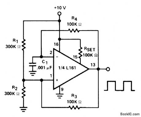
View full Circuit Diagram | Comments | Reading(0)
SET_TESET_LATCH
Published:2009/7/6 7:23:00 Author:May
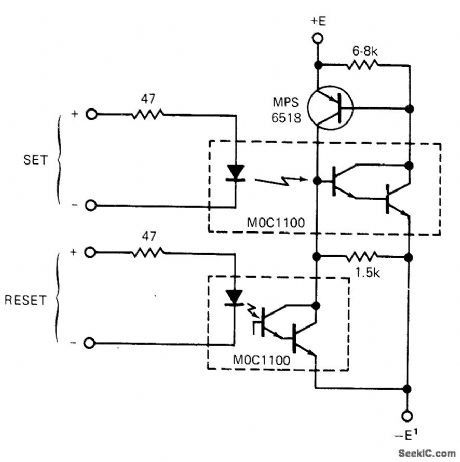
Provides almost complete isolation between each input and the output, as well as between inputs. Applying 2-V pulse at 14 mA momentarily to SET terminals allows up to 150 mA to flow between output terminals. This current flows until about 2 V at 15 mA is appkied to REST terminals or untilload voltage is reduced enough to drop load current below 1 mA.-R.N. Dotson, Set-Reset Latch Uses Optical Couplers, EDN Magazine, Jan.5, 1973, p 107. (View)
View full Circuit Diagram | Comments | Reading(620)
OPTOISOLATOR_INPUT_PROTRCTION
Published:2009/7/6 7:19:00 Author:May
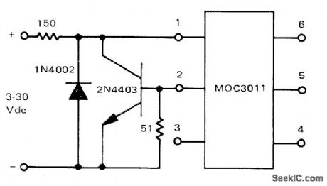
Combination of diode and transistor limits input current to LED of Motorola MOC3011 optoisolator to safe maximum of less than 15 mA for input voltage range of 3-30 VDC. Circuit also protects LED from accidental reversal of polarity.-P.O 'Neil, “Applications of the MOC3011 Triac Driver,” Motorola, Phoenix, AZ, 1978, AN-780, p 4. (View)
View full Circuit Diagram | Comments | Reading(640)
DC_ISOLATOR_WITH_HARMONIC_SUPPESSION
Published:2009/7/6 7:19:00 Author:May
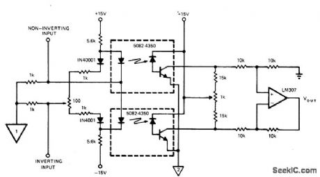
Two isolators operating like push-pull amplifier minimize harmonic generation. When input signal is applied, upward change of incremental gain in one isolator is balanced by downward change in other to give harmonic cancellation. Circuit gain is about unity. Bandwidth is 2 MHz for signal below 2 V p-p. Input signals of either polarity may be applied at either inverting or noninverting input.-H. Sorensen, Opto-Isolator Developments Are Making Your Design Chores Simpler, EDN Magazine, Dec. 20, 1973, p 36-44. (View)
View full Circuit Diagram | Comments | Reading(639)
OPTICAL_DRIVE_FOR_SWITCHING_TRANSISTOR
Published:2009/7/6 7:17:00 Author:May
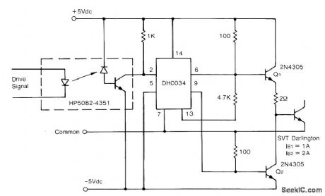
Base driver circuit for TRW SVT6062 power Darlington switching transistor uses separate isolated bias supplies for each transistor to provide performance characteristics of driver transformer at lower cost. Bias supplies can use small 60-Hz transformers with bridge rectifiers and light filtering. Control isolation is provided by high-speed optical coupler that can be controlled directly from logic. DH0034 IC amplifies coupler output and provides level shifting as required for driving transistors Q1 and Q2.-D. Roark, Base Drive Considerations in High Power Switching Transistors, TRW Power Semiconductors, Lawndale, CA, 1975, Application Note No. 120, p 8. (View)
View full Circuit Diagram | Comments | Reading(939)
CMOS_555_ASTABLE_GENERATES_TRUE_RAIL_TO_RAIL_SQUARE_WAVES
Published:2009/7/6 7:15:00 Author:May
A CMOS timer generates true square waves because, unlike the bipolar 555, its output swings from rail to rail. The component values shown give a frequency of about 400 Hz.
(View)
View full Circuit Diagram | Comments | Reading(919)
PULSE_AMPLIFIER
Published:2009/7/6 7:15:00 Author:May
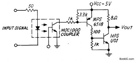
Motorola MOC1000 optoisolator permits coupling digital logic to system having different supply voltages or unequal grounds while providing essentially complete isolation. Circuit provides transfer characteristics needed in instrumentation applications and has sufficient drive for handling low input impedances.- Industrial Control Engineering Bulletin, Motorola, Phoenix, AZ, 1973, EB-4. (View)
View full Circuit Diagram | Comments | Reading(929)
FAST_OPTICALLY_ISOLATED_SWITCH
Published:2009/7/6 7:14:00 Author:May
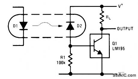
Uses almost any standard optoisolator. Less than 20μA is needed from photodiode D2 to tum LM195 power transistor fully on. Returning cathode of D2 to separate positive supply rather than to collector of al eliminates collector-base capacitance of diode and increases switching speed to 500 ns for 40-V 1-A load.-R. Dobkin, Fast IC Power Transistor with Thermal Protection, National Semiconductor, Santa Clara, CA, 1974, AN-110, p 5. (View)
View full Circuit Diagram | Comments | Reading(815)
OSCILLATOR_WITH_FREQUENCY_DOUBLED_OUTPUT
Published:2009/7/6 7:14:00 Author:May
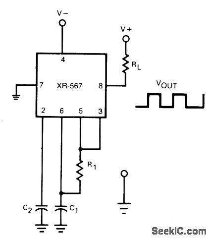
The current-controlled oscillator frequency can be doubled by applying a portion of the square-wave output at pin 5 back to the input at pin 3, as shown. In this manner, the quadrature detector functions as a frequency doubler and produces an output of 2 f0 at pin 8. (View)
View full Circuit Diagram | Comments | Reading(469)
Digital Multimeter Electric Block Circuit with Constant Current Source
Published:2011/7/27 10:10:00 Author:Michel | Keyword: Digital Multimeter, Block Circuit, Constant Current Source
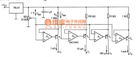
The digital multimeter electric block diagram with constant current source is shown as above.The electrical resistance measuring principle in the digital multimeter is that measured resistance is used to generate voltage with constant current.Constant current source adopts 4 op-amp MC3403,UREF=1V is set by RP1 (2 Ok Ω resistance).The constant current output is IREF=UREF/Rs,thus,when Rs=1MΩ,IZ is 1μA,when Rs=1OOkΩ,IY is 10μA,when Rs=1OkΩ,IX is 100μA and Iw is 1 mA when Rs=1kΩ. (View)
View full Circuit Diagram | Comments | Reading(1765)
DC_DC_OPTOISOLATOR
Published:2009/7/6 7:14:00 Author:May
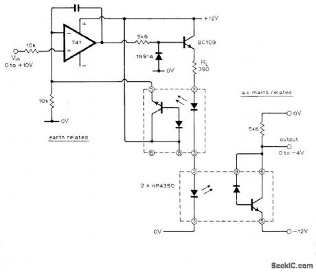
Designed to provide input isolation for thyristor converters. Linearity is within 2%. Loop gain of opamp makes diode turn-on voltage insignificant.-R. J. Haney, Linear D.C./D.C. Opto Isolator, Wireless World, June 1976, p 72. (View)
View full Circuit Diagram | Comments | Reading(972)
BAR_CODE_READER
Published:2009/7/6 7:13:00 Author:May

Edge-sensitive circuit outputs short pulses at each black-to-white or white-to-black transition. Timing diagram shows outputs corresponding to bar-code pat-tern indicated. Direct-current level at base of Q1 is held constant by DC servo action despite changes in temperature, ambient light, or back-ground of pattern. Alternate sensor uses photodiode and 2N2222 transistor for increased bandwidth. Amplified differentiated signal from collector of a2 is further amplified by IC2 and fed to dual threshold comparator. Output of comparator is short pulse for each transition, suitable for feed to microprocessor.-F. L. Merkowitz, Signal Processing for Optical Bar Code Scanning, BYTE, Dec. 1976, p 77-78 and 80-84. (View)
View full Circuit Diagram | Comments | Reading(4293)
SQUARE_WAVE_GENERATOR_USING_A_555_TIMER
Published:2009/7/6 7:12:00 Author:May
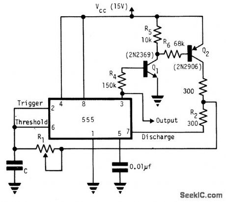
A single timing resistor ensures that the output is a square (50% duty cycle) wave at at all frequency settings. (View)
View full Circuit Diagram | Comments | Reading(1307)
LOW_FREQUENCY_TTL_OSCILLSATOR
Published:2009/7/6 7:11:00 Author:May
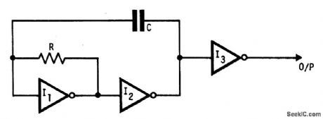
This oscillator uses standard inverters,one resistor and one capacitor,and has nommmlum operating frequency.R and C must be chosen such that currents into the gatesare below recommended operating limits and that leakage current into the gates andinto C are small h companson with the current in R also the output should be buffered(I3)to prevent variations h load affecting frequency.This circuit may also be used to square up slowly changing logic levels by use of multi input gates (NANDS,NORS Etc). (View)
View full Circuit Diagram | Comments | Reading(617)
FULL_WAVE_RECTIFIER
Published:2009/7/6 7:11:00 Author:May
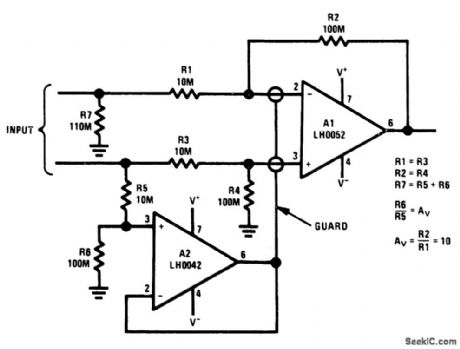
Circuit provides accurate full-wave rectification of input signal, with distortion below 5% up to 10 kHz. Reversal of all diode polarities reverses polarity of out-put. Output impedance is low for both input polarities, and errors are small at all signal levels.- Signetics Analog Data Manual, Signetics, Sunnyvale, CA, 1977, p 641-643. (View)
View full Circuit Diagram | Comments | Reading(905)
COMPLEMENTARY_POSTAMPLIFIER
Published:2009/7/6 7:10:00 Author:May
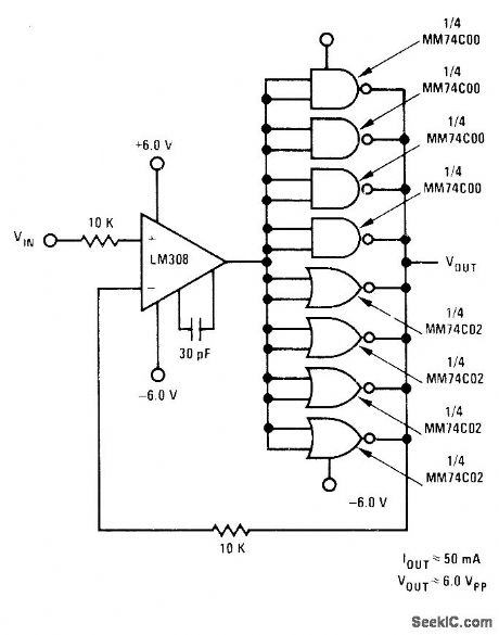
Paralleled NAND gates provide buffering for LM308 opamp while increasing current drive to about 50 mA for 6 V P-P output,MM74C00 NAND gates supply about 10 mA each from positive supply while MM74C02 gates supply same amount from negative supply.- Linear Applications, Vol. 2, National Semiconductor, Santa Clara, GA, 1976, AN-88, p 2-3. (View)
View full Circuit Diagram | Comments | Reading(526)
P012404UD Frequency Synthesizer Integrated Circuit
Published:2011/7/27 9:55:00 Author:Michel | Keyword: Frequency Synthesizer, Integrated Circuit
P012404UD is a kind of frequency synthesizer integrated circuit which is widely used in samsung mobile phones, such as CDMA series samsung A599 cell phones, etc.
First,Functions FeaturesPO12404UD integrated circuit contains the second phase lock voltage circuit,second vibration vibration power supply circuit, data circuit, frequency synthesis start-up circuit, reference frequency circuit and some auxiliary function circuit.
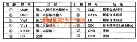
Second,Pins FunctionsPO12404UD integrated circuits uses 12 feet 4 columns encapsulation.And pins functions of frequency synthesis clock circuit and its integrated circuit are shown as table 1.
Table 1:PO12404UD IC Pins Functions (View)
View full Circuit Diagram | Comments | Reading(419)
_FUNK_BOX
Published:2009/7/6 7:10:00 Author:May
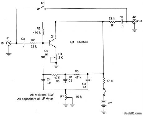
Adjusting potentiometer R7 adds extra twang from way down low to way up high.To set the unit,adjust potentiometer R4 until you hear a whistle (oscillation); then back off R4 until the oscillation just ceases. The effect can be varied from bass to treble by R7.
(View)
View full Circuit Diagram | Comments | Reading(489)
STEAM_TRAIN_PROP_PLANE
Published:2009/7/6 7:08:00 Author:May
View full Circuit Diagram | Comments | Reading(804)
| Pages:1035/2234 At 2010211022102310241025102610271028102910301031103210331034103510361037103810391040Under 20 |
Circuit Categories
power supply circuit
Amplifier Circuit
Basic Circuit
LED and Light Circuit
Sensor Circuit
Signal Processing
Electrical Equipment Circuit
Control Circuit
Remote Control Circuit
A/D-D/A Converter Circuit
Audio Circuit
Measuring and Test Circuit
Communication Circuit
Computer-Related Circuit
555 Circuit
Automotive Circuit
Repairing Circuit