
Circuit Diagram
Index 1023
8_bit_D_A_converter_with_microprocessor_interface
Published:2009/7/23 21:39:00 Author:Jessie

This circuit uses a DAC-4881 and a few external components to form a D/A converter with microprocessor interface (8-bit data bus). The output is + 10 V to -10 V with complementary binary input (all zeros equal full scale). (View)
View full Circuit Diagram | Comments | Reading(833)
Constant_voltage_crossover_network
Published:2009/7/23 21:11:00 Author:Jessie

This active crossover network provides 12-dB/octave slopes, where the crossover frequency is determined by: 1/(6.28RC). Figure 1-46B shows both the low-pass and high-pass responses, with a crossover frequency of 1kHz. Notice that the summed response (dashed lines) is perfectly flat. (View)
View full Circuit Diagram | Comments | Reading(1422)
Multiple_line_driver_buffer
Published:2009/7/23 21:11:00 Author:Jessie
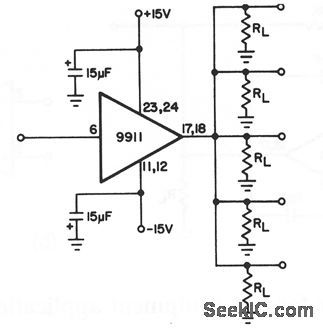
This circuit shows a 9911 used as a driver for multiple lines, which allows a video signal to be routed to 5 (or more) individual directions. A typical application is an apartment building with a common cable system. Although the 9911 is capable of 500-mA drive at a± 10-V output voltage swing, this application usually does not require more than± 1 or±2 V (for a typical video system). This circuit can be inexpensive because only one voltage-follower/buffer and few external components are needed. (View)
View full Circuit Diagram | Comments | Reading(641)
Simple_fast_10_bit_A_D_converter
Published:2009/7/22 21:59:00 Author:Jessie

This circuit is especially useful where a large number of converters is required and all can be serviced by one clock. For a 0-2.5-V range, the analog input (EX) is applied to the 2.5-kΩ resistor. For a 0-to 10-V range, the 2.5-kΩ resistor is grounded and EX is applied to the 7.5-kΩ resistor. The 100-MHz clock pulse bursts that appear at the output are proportional to EX. For a 0- to 10-V input, 1024 pulses appear at full-scale, 512 pulses at 5.00 V etc. The circuit will hold ±1 LSB accuracy over 0°C to 70°C with an additional t1 LSB uncertainty. The 2-kΩ gain trim pot is adjusted for the desired output count. (View)
View full Circuit Diagram | Comments | Reading(990)
Optocoupler_that_is_used_to_couple_ac_to_an_op_amp
Published:2009/7/22 21:59:00 Author:Jessie
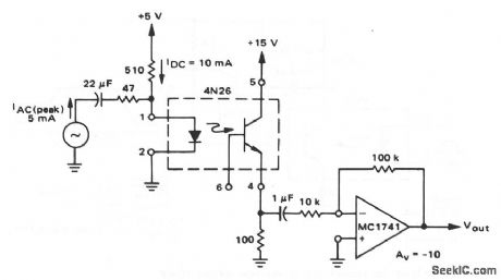
In this circuit, the LED portion of the 4N26 is biased with a dc current of 10 mA. The input ac signal is summed with the dc bias so that the 4N26 output has both ac and dc components. Because the op amp is capacitively coupled to the 4N26, only the ac signal appears at the op-amp output. (View)
View full Circuit Diagram | Comments | Reading(3191)
Fully_isolated_10_bit_A_D_converter
Published:2009/7/22 21:56:00 Author:Jessie

This circuit is fully floating from system ground, and is ideal for performing A/D conversion in the face of the high common-mode noise characteristics of predominantly digital systems. The circuit is also useful in industrial environments where noise and high common-mode voltages are present in transducer-fed systems. To calibrate, apply 3.000 V at the input, and trim the 5-kΩ pot for 1024 counts at the data output (Q4 collector). (View)
View full Circuit Diagram | Comments | Reading(767)
Microporoer_12_bit_A_D_converter
Published:2009/7/22 21:53:00 Author:Jessie

This A/D converter has a 300-μs conversion time, consumes only 890 μA, with a temperature coefficient of 30 ppm/°C and an accuracy of ±2 LSBs. To calibrate, adjust the 100-kΩ pot for exactly -5V at VREF (pin 5 of the LTC1044). No further adjustment is necessary. (View)
View full Circuit Diagram | Comments | Reading(918)
Optocoupler_that_is_used_as_a_load_to_logic_translator
Published:2009/7/22 21:52:00 Author:Jessie

This circuit shows a 4N26 that is used to couple a high-voltage load to a low-voltage logic input. In this case, the value of R is chosen so that the output current is greater than 10 mA (to ensure that the 4N26 output voltage exceeds the logic-one level of the flip-flop). (View)
View full Circuit Diagram | Comments | Reading(1716)
Low_cost_high_level_preamp_and_tone_control
Published:2009/7/22 20:19:00 Author:Jessie

This circuit uses the JFET to best advantage (low impedance). All device parameters are non-critical, yet the circuit achieves harmonic distortion of less than 0.05% with a S/N ratio of over 85 dB. The tone controls allow 18-dB of cut and boost. The amplifier has a 1-V output for 100-mV input at maximum level. (View)
View full Circuit Diagram | Comments | Reading(1257)
Optoisolator_driver_for_resistive_loads
Published:2009/7/22 6:02:00 Author:Jessie
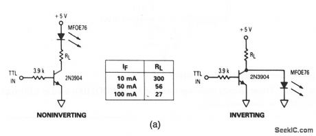

These circuits show a visible red LED (MFOE76) that is used as fiberoptic drivers for both noninverting and inverting TTL inputs. Figure 9-34B shows typical fiberoptic termination and assembly for both receivers and transmitterS. (View)
View full Circuit Diagram | Comments | Reading(946)
Battery_powered_12_volt_5_MHz_frequency_counter_using_McMOS_logic
Published:2009/7/22 5:43:00 Author:Jessie

Battery powered (12-volt) 5 MHz frequency counter using McMOS logic (cour tesy Motorola Semiconductor Products Inc.).
(View)
View full Circuit Diagram | Comments | Reading(743)
9_digit_multifunction_counter_using_the_Intersil_ICM7226A_40_pin_DIP
Published:2009/7/22 5:36:00 Author:Jessie
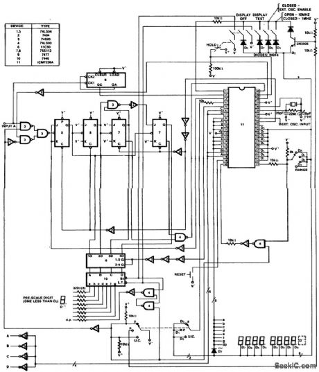
9-digit multifunction counter using the Intersil ICM7226A 40-pin DIP (courtesy Intersil, Inc.). (View)
View full Circuit Diagram | Comments | Reading(787)
I2C Bus Control Storage Integrated Circuit of PCF8582
Published:2011/7/28 22:40:00 Author:Michel | Keyword: I2C Bus, Storage Integrated Circuit

PCF8582 is the I2C bus control electrically erasable/programming read-only memory integrated circuits, which is widely used in big TV screens and other video, audio, air conditioner microcomputer control system.
First,Functions Features
PCF8582 integrated circuit contains erasable/programmable read-only memory case, the I2C bus control interface and address signals interface circuits, etc.
Second,Pins Functions and Data
PCF8582 integrated circuit adopts feet 8 DIP package and its pins functions and data are shown as the table 1.
Table 1 :PCF8582 Pins Functions and Data (View)
View full Circuit Diagram | Comments | Reading(769)
emperature_controller_that_uses_zero_point_switching
Published:2009/7/22 4:21:00 Author:Jessie
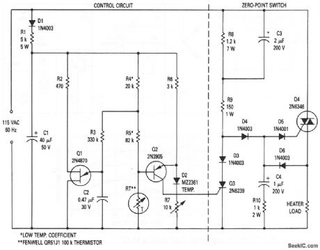
This circuit shows the basic UJT building block (Fig. 9-1), which is used to control a zero-point switching temperature controller. The circuit applies the correct amount of power on a continuous basis at a steady-state duty cycle, depending on the load requirements. Temperature is therefore controlled over a very narrow range and no EMI is generated, The temperature is set by R7. (View)
View full Circuit Diagram | Comments | Reading(640)
4_decade_synchronous_counter_with_data_display_multiplexing
Published:2009/7/22 4:17:00 Author:Jessie
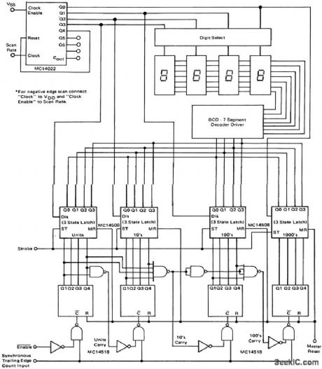
4-decade synchronous counter with data display multiplexing (courtesy Motorola Semiconductor Products Inc.). (View)
View full Circuit Diagram | Comments | Reading(728)
90_V_voltage_regulator_that_uses_a_PUT
Published:2009/7/22 4:17:00 Author:Jessie
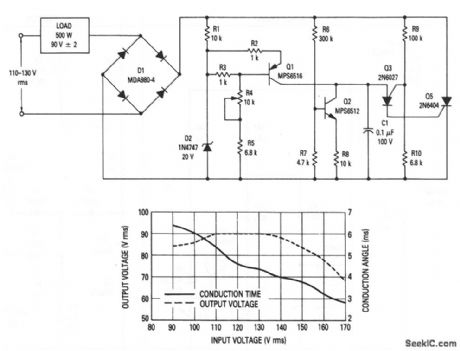
This circuit shows a PUT that is used to control a voltage regulator. Figure 9-28B shows a plot of output voltage and conduction angle versus input voltage for the regulator. The output voltage is set by R4. (View)
View full Circuit Diagram | Comments | Reading(612)
Battery_charger_that_uses_a_PUT
Published:2009/7/22 4:14:00 Author:Jessie
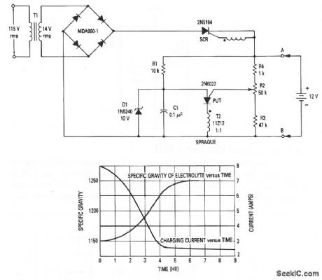
This circuit shows a PUT that is used to control a short-circuit-proof battery charger. Figure 9-27B shows the charging characteristics of the circuit. The charger provides an average charging current of about 8 A to a 12-V lead-acid storage battery. The circuit will not function or will be damaged by improperly connecting the battery because battery current is used to charge timing capacitor C1 (the SCR remains cut off, and the PUT relaxation oscillator does not function until a battery is connected as shown). The maximum battery voltage (10 to 14 V) is set by R2. (View)
View full Circuit Diagram | Comments | Reading(1644)
Discrete_component_audio_amplifier_7_to_35_W_pnp_driver
Published:2009/7/22 4:11:00 Author:Jessie


This circuit provides a 1- to 35-W output, depending on power source and component values (as shown), with overload protection. Figures 1-19B and 1-19C show the PC-board layout and performance characteristics, respectively. (View)
View full Circuit Diagram | Comments | Reading(1108)
SPEECH_NETWORK
Published:2009/7/6 20:49:00 Author:May

The XR-T5995 Speech Network is a monolithic integrated circuit specifically designed for implementing a low cost telephone circuit. It is designed to use an electrodynamic microphone and electromagnetic receiver to replace a carbon microphone and telephone network hybrid.
(View)
View full Circuit Diagram | Comments | Reading(6105)
GRAPHICS_INTERFACE
Published:2009/7/6 20:49:00 Author:May
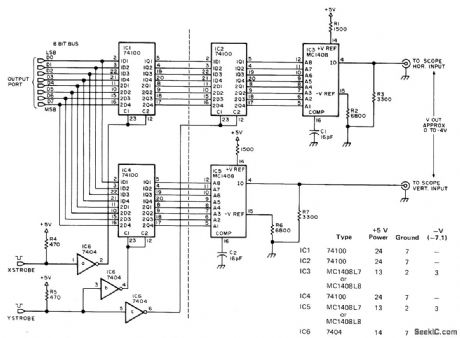
Used between computer and ordinary CRO to create images with array of 512 x 512 dots stored in computer memory. Location of each dot is specified by two voltages, for application to V and H inputs of CRO. Computer provides voltage values by outputting two binary words to pair of DACs giving voltages proportional to numerical values of words. Dot pattern is repeated many times per second to give steady nonflickering image. Dot brightness can be increased by storing in several locations so it is refreshed more often than other points. Article gives listing for Intel 8080 graphics drive program. Program pro-vides for interrupts once per scan to give key-board-controlled drawing mode,-P. Nelson, Build the Beer Budget Graphics Interface, BYTE, Nov. 1976, p 26-29. (View)
View full Circuit Diagram | Comments | Reading(647)
| Pages:1023/2234 At 2010211022102310241025102610271028102910301031103210331034103510361037103810391040Under 20 |
Circuit Categories
power supply circuit
Amplifier Circuit
Basic Circuit
LED and Light Circuit
Sensor Circuit
Signal Processing
Electrical Equipment Circuit
Control Circuit
Remote Control Circuit
A/D-D/A Converter Circuit
Audio Circuit
Measuring and Test Circuit
Communication Circuit
Computer-Related Circuit
555 Circuit
Automotive Circuit
Repairing Circuit