
Circuit Diagram
Index 545
TDA1020 12W Audio power amplifier circuit diagram
Published:2011/8/22 22:14:00 Author:Rebekka | Keyword: 12W, Audio power amplifier
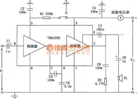
View full Circuit Diagram | Comments | Reading(1819)
TDA1102 20WHi-Fi Power amplifier circuit diagram
Published:2011/8/22 22:14:00 Author:Rebekka | Keyword: 20WHi-Fi, Power amplifier

View full Circuit Diagram | Comments | Reading(1275)
Comprehensive protector belt circuit composed of 555
Published:2011/8/22 22:09:00 Author:Rebekka | Keyword: Comprehensive protector belt, 555

Start upcircuit is composed of the start button QA, IC1 (555), IC2 (555), J1 and so on. When you press the QA, the +12 V voltage output by the buck rectifier circuit will be added to IC1, IC2, then relay J1 will be pulled. It also starts the bell ring. When it adds a +12 V voltage, the IC1 is set aspin potential of pin ② is low (the voltage on C1can not mutate), and C1 charges for R1, when the C1 charges to make IC1 ⑥ potential higher than 2 feet / 3VDD, IC1 will be reset. (View)
View full Circuit Diagram | Comments | Reading(952)
Composition of F033 the photosensitive signal amplifying circuit diagram
Published:2011/8/22 22:13:00 Author:Rebekka | Keyword: Photosensitive Signal

Sensitive signal amplification circuitis used toamplify photodiode or phototransistor optoelectronic devices such as electrical signals. When the incident light illumination changes, the optical devicecan generate certain current, because the signal is very weak sensitive, so it’s better to use a operational amplifier in very low input bias current. In order to eliminate oscillations, it adds a small capacitor C (pF orders of magnitude) in the feedback circuit, but the value of C affects the bandwidth of the amplifier. The DC gain of the circuit is l00, 1000,10000, you can select switch corresponding to 10kΩ, 1kΩ, 100Ω resistors to ground, the circuit of the resistor accuracy must be better than ± 1%. Photocell uses FPT102 or FPT100. (View)
View full Circuit Diagram | Comments | Reading(588)
Op amp power supply decoupling bypassing measure circuit diagram
Published:2011/8/22 22:12:00 Author:Rebekka | Keyword: Op amp power supply, decoupling bypassing measure

Each power lead of the integrated power amplifier generally uses decoupling bypassing measure. That means connecting a high-performance capacitor from power lead end to extend across. It is shown in the figure. The high frequency bypass capacitor shown in the figure usually chooses a high performance ceramic capacitor, its value is 0.1μF. It can also use lμF tantalum capacitor. The internal inductance of these capacitors are small. When the op amp works in a high-speed, the bypass capacitors C1 and C2 should be connected to the power supply pins of integrated amplifier. The leads should be as short as possible to form a low inductance ground return circuit. When the gain-bandwidth of the used amplifier is greater than 10MHz, you should adopt more stringent high-frequency bypass measures. (View)
View full Circuit Diagram | Comments | Reading(3033)
Op amp input compensation capacitor circuit diagram
Published:2011/8/22 22:12:00 Author:Rebekka | Keyword: Op amp, input compensation capacitor
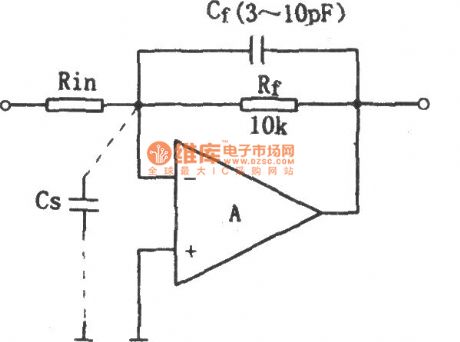
General linear amplifier (namely the work of the negative feedback amplifier circuit) input parasitic capacitance will influence the stability of Cs circuit, the compensation measures are shown in the map. The amplifier's input generally exists a few parasitic capacitance Cs. The Cs includes op-amp input capacitance and wiring distributed capacitance. Its feedback resistor Rf can form a lag network and cause output voltage phase lag. When the input signal frequency is high, the bypass action of the Cs makes the amplifier's high frequency response become worse, the frequency band of the upper limit of frequency is about: Omega h = 1 / (2 PI RfCs) . (View)
View full Circuit Diagram | Comments | Reading(4579)
Basic inverting amplifier circuit composed of the μA709
Published:2011/8/22 22:10:00 Author:Rebekka | Keyword: Basic inverting amplifier
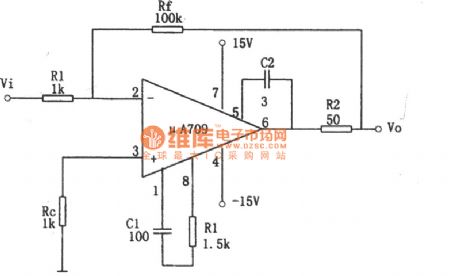
The figure of the basic inverting amplifier circuit composed of the μA709 is shown as above.
The main performance of the U A709 :
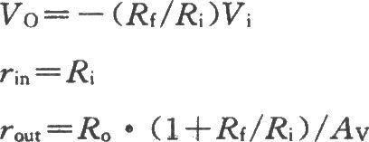
According to the figure, the feedback resistor Rf will connect the output and input ends. Since the circuit output, input voltage are inverting, the Rf leads the voltage parallel negative feedback. Thereby the amplifier works in linear region with the op-amp transmission characteristics, that is, the output voltage is proportional to the input voltage. In addition, the inverting input end is connected to the resistor Ri in series, and it is the operational amplifier's input resistor. The increasing of Ri can reduce the source of the load.
(View)
View full Circuit Diagram | Comments | Reading(987)
High-speed programmable gain amplifier circuit composed of the INA110
Published:2011/8/12 4:23:00 Author:Rebekka | Keyword: High-speed , programmable gain amplifier

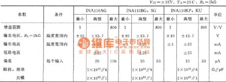
The figure shows the high-speed programmable gain amplifier circuit. The main circuit is composed of the rapid and stable instrument integration op-amp INA110. Because the INA110 builds time fast, so it is the ideal amplifier circuit for the high speed or multiple data acquisition system. When the gain Av = 100, its build time can be up to 3 us.
(View)
View full Circuit Diagram | Comments | Reading(1014)
M5112Y 5W Audio power amplifier circuit diagram
Published:2011/8/12 4:20:00 Author:Rebekka | Keyword: 5W, Audio power amplifier

M5112Y is 5W audio power amplifier integrated circuit. The circuit output power is large, less distortion, wide frequency bandwidth. It is suitable for car radio and stereo audio power amplifier device for stereo audio power amplifier. M5112Y 5W Audio power amplifier circuit diagram is shown as below.
(View)
View full Circuit Diagram | Comments | Reading(2758)
M51304L Microphone amplifier circuit diagram
Published:2011/8/12 4:20:00 Author:Rebekka | Keyword: Microphone amplifier
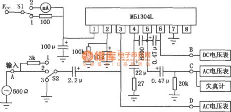
M51304L is microphone amplifier circuit. It uses 8-pin single inline package. The power supply voltage is 8~15V with low noise. There is automatic gain control (AGC) circuit inside. You can adjust the sensitivity of agc though external resistor. It is suitable for the microphone amplifier of micro recorder. The typical application circuit diagram is shown as below.
(View)
View full Circuit Diagram | Comments | Reading(2300)
M51513L 5.8W Audio power amplifier circuit diagram
Published:2011/8/15 2:17:00 Author:Rebekka | Keyword: 5.8W, Audio power amplifier
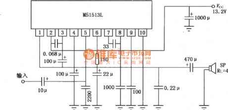
M51513L is theaudio power amplifier IC. It uses 10-pin single in-line plastic package. The features of the two ICs are high voltage gain, large output power and they even work in 2Ω load. The power supply voltage is 9~16V. The output power is 5.8W(Typical), when the power supply voltage is 13.2V, load impedance is 4Ω and distortion is 10%. There are short-circuit protection, thermal cut off, power surge voltage protection etc. in the circuit. It is suitable for the audio power amplifier of car radio, car stereo installation. The typical application circuit of M51513L is shown as below.
(View)
View full Circuit Diagram | Comments | Reading(4001)
Sawtooth wave generating circuit composed of the LM747
Published:2011/8/14 19:45:00 Author:TaoXi | Keyword: Sawtooth wave, generating
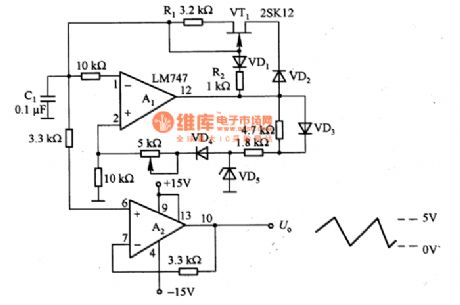
The sawtooth wave generating circuit which is composed of the LM747 is as shown in the figure. It uses the self-excited multivibrator to produce the sawtooth wave. In order to make the capacitance C1's chargig voltage line increase linearly, we use the constant current source which is composed of the VT1 and R1. And in order to reduce return time of the sawtooth wave, the VD1 and R2 supply the discharging circuit which has very small discharge time constant. The voltage-regulator diode VD5 clamps the output of A1 to stabilize the output amplitude of it. When the C1 is discharging, if you supply the reverse bias to the VD5, the VD4 will cut off, the in-phase input port of A1 is 0V, the minimum level of the sawtooth wave goes back to 0V.
(View)
View full Circuit Diagram | Comments | Reading(1829)
RC type scanning signal generator circuit composed of the FET tube
Published:2011/8/14 20:13:00 Author:TaoXi | Keyword: RC type, scanning signal, generator, FET tube


The RC type scanning signal generator circuit which is composed of the FET tube is as shown in the figure. This circuit is the Wien bridge RC oscillation circuit, and it is composed of the oscillation amplifier and the positive and negative feedback circuit. The oscillation frequency is decided by the RC value of the positive feedback circuit, now we suppose C=O.001μF to calculate the resistance of resistor R to see whether it meet the requirements.
The scanning circuit is composed of the constant current source, the constant current charging capacitor and the scanning discharging circuit, the VT10 constant current source charges the capacitors C3 - C5, when the charging voltage of the capacitor gets to a certain value, it will be compared by the comparator through the A2.
(View)
View full Circuit Diagram | Comments | Reading(1013)
AC power supply monitoring circuit composed of the 74HC123
Published:2011/8/14 20:27:00 Author:TaoXi | Keyword: AC, power supply, monitoring

The AC power supply monitoring circuit composed of the 74HC123. When the AC power is cut off, the important data that is storaged in the microcomputer might disappear. So we need to add the power transient breaking detection circuit to protect the data in the memorizer. The AC220V voltage is rectified and stabilized to be the +5V ouptut voltage, the voltage can be used as the operating power of the microcomputer, and also it is the operating power of the timer 74HC123 (the 13-pin of the 74HC123 is connected with the microcomputer). When the AC power is normal, the 74HC123 timer will reset to output the high level, the microcomputer operates normally.
(View)
View full Circuit Diagram | Comments | Reading(2116)
Controllable conversion rate circuit
Published:2011/8/14 21:31:00 Author:TaoXi | Keyword: Controllable, conversion rate

The controllable conversion rate circuit is as shown in the figure. It controls the conversion rate by adjusting the signal rising velocity, if it is used in the system which use the voltage signal to control the motor speed, it can control the deceleration and acceleration of the motor. The comparator circuit is composed of A1, the amplitude limiting circuit is composed of the VD1 and VD2. The conversion rate is decided by the VD1 and VD2's positive voltage drops and the product of the (R(RP1)+R1) and Cl, the larger the values of R(RP1), R1 and Cl, the smaller the conversion rate is.
(View)
View full Circuit Diagram | Comments | Reading(548)
The circuit uses the pulse width modulation mode to control the load
Published:2011/8/14 22:09:00 Author:TaoXi | Keyword: pulse width, modulation mode, load

The circuit that uses the pulse width modulation mode to control the load is as shown in the figure. The oscillation frequency of the circuit is decided by the Rl+R(RP1) and C1, f=1/[2·2(Rl+R(RP1)Cl]. The waveform duty cycle is decided by the (Rz+R(RP2)) and C2. The optocoupler TLP5llGA has the electrical isolation effect for the output and input, so the output can use the 220V AC high voltage power supply. The LED can be used to display the changes of the duty cycle.
(View)
View full Circuit Diagram | Comments | Reading(772)
Electric fan infrared remote control circuit (6)
Published:2011/8/11 19:45:00 Author:TaoXi | Keyword: Electric fan, infrared, remote control
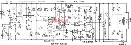
infrared transmitter
(View)
View full Circuit Diagram | Comments | Reading(1214)
AN5071 frequency band switching control integrated circuit
Published:2011/8/11 19:53:00 Author:TaoXi | Keyword: frequency band, switching, control, integrated circuit


The AN5071 is designed as the frequency band switching control integrated circuit which is produced by the Panasonic company, and it can be used in all kinds of screen color TV sets.
1. The internal circuit block diagram
The AN5071 has three channels of electronic switch and the 30V voltage-stabilizing circuit, the internal circuit block diagram of the manifold is as shown in figure 1-15.
2.Pin functions and data
The AN5071 uses the 9-pin single row package, the pin functions and data of the integrated circuit is as shown in table 1-14.
Table 1-14 The pin functions and data of the AN5071 (View)
View full Circuit Diagram | Comments | Reading(1554)
Electric fan infrared remote control governor circuit
Published:2011/8/11 20:00:00 Author:TaoXi | Keyword: Electric fan, infrared, remote control, governor

The electric fan infrared remote control governor circuit is as shown in the figure. (View)
View full Circuit Diagram | Comments | Reading(1142)
Electric fan infrared remote control speed control switch circuit
Published:2011/8/11 20:08:00 Author:TaoXi | Keyword: Electric fan, infrared, remote control, speed control switch


Emitter:
Receiver:
(View)
View full Circuit Diagram | Comments | Reading(857)
| Pages:545/2234 At 20541542543544545546547548549550551552553554555556557558559560Under 20 |
Circuit Categories
power supply circuit
Amplifier Circuit
Basic Circuit
LED and Light Circuit
Sensor Circuit
Signal Processing
Electrical Equipment Circuit
Control Circuit
Remote Control Circuit
A/D-D/A Converter Circuit
Audio Circuit
Measuring and Test Circuit
Communication Circuit
Computer-Related Circuit
555 Circuit
Automotive Circuit
Repairing Circuit