
Circuit Diagram
Index 553
Double-digit display seconds timer circuit diagram
Published:2011/8/11 2:23:00 Author:Rebekka | Keyword: Double-digit display , seconds timer
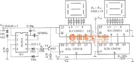
Double-digit display seconds timer(5G5544、CD4511、CD4518) circuit diagram is shown as above.
The maximum time timer of explicit two-digit seconds is 99s. The circuit is composed of a time-base signal which is quartz clock IC 5G5544 output pulse signal. Since the pulse period of circuit output is 2s, it achieves the seconds output functionby matchingwith transistor VT and two input ends of the counter. (View)
View full Circuit Diagram | Comments | Reading(3174)
AN7100S Two-track audio power amplifier circuit diagram
Published:2011/8/11 2:44:00 Author:Rebekka | Keyword: Two-track , audio power amplifier
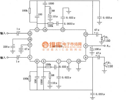
AN7100S is two-track audio power amplifier circuit diagram, which uses dual flat package. Its working power supply voltage is 1~3V. The circuit hasthe advantages of lowquiescent current, low noise and small distortion. It is suitable for 1.5V power supply voltage tape recorders. The max power supply voltage is VCC=3V. Power dissipation PD=60mW is available. The typical application circuit diagram is shown as below.
(View)
View full Circuit Diagram | Comments | Reading(2129)
AN7113S Audio power amplifier circuit diagram
Published:2011/8/11 2:21:00 Author:Rebekka | Keyword: audio power amplifier
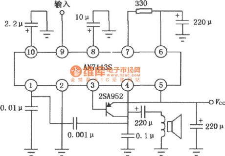
AN7113S is an audio power amplifier circuit with 10-pin dual flat package. The working power supply voltage is 1.8~4.5V. There isfew external components in the circuit. Its quiescent current can be adjusted by different loads. The circuit is suitable for low micro-radio or the power amplifier of tape recorders. The max power supply voltage of AN7113S is VCC=4.5V. Power dissipation PD=360mW(T=25℃) is available. AN7113S Audio power amplifier circuit diagram is shown as below.
(View)
View full Circuit Diagram | Comments | Reading(2618)
The typical application circuit diagram of AN102S dual track audio power amplifier
Published:2011/8/12 3:28:00 Author:Rebekka | Keyword: typical application , dual track , audio power amplifier

View full Circuit Diagram | Comments | Reading(906)
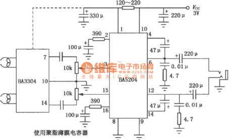
BA5204/5204F 3V Two-track audio power amplifier typical application circuit diagram
Published:2011/8/12 4:20:00 Author:Rebekka | Keyword: 3V, typical application , Two-tracll audio power amplifier
View full Circuit Diagram | Comments | Reading(1604)
CX20172 Two-track audio power amplifier circuit diagram
Published:2011/8/12 4:19:00 Author:Rebekka | Keyword: Two-track , audio power amplifier

CX20172 uses 14-pin dual flat package, operating supply voltage 0.9 ~ 2.2V. when Vcc is 1.5V, RL is 8Ω and THD is 10% the two-channel in the working mode. Every output channel power is 20mW. BTL connection output power is 80mW. There is not mute and power off function in circuit. The max power supply voltage is Vcc=4.5V and power dissipation PD=560mW(TA=25℃) is available. CX20172 Two-channel audio power amplifier circuit diagram is shown as below.
(View)
View full Circuit Diagram | Comments | Reading(1104)
HA1388 18W BTL Audio power amplifier circuit diagram
Published:2011/8/12 4:18:00 Author:Rebekka | Keyword: 18W BTL , Audio power amplifier
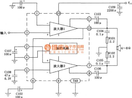
HA1388 is an audio power amplifier IC. It uses 12-pin single in-line plastic package structure. The output power is 18W without output coupling capacitor when the supply voltage is 13.2V, 4Ω load impedance and 10% distortion. Thereis overvoltage and thermal shutdown protection in the circuit and fewer external components. The audio Power Amplifier is suitable for car radio. HA1388 Internal circuit diagram and typical application circuit are shown as below.
(View)
View full Circuit Diagram | Comments | Reading(4032)
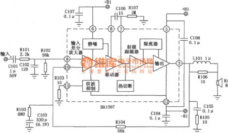
20W Audio power amplifier HA1397 typical application circuit diagram
Published:2011/8/12 4:18:00 Author:Rebekka | Keyword: typical application, Audio power amplifier
View full Circuit Diagram | Comments | Reading(3758)
LA4230/4250 8W Audio power amplifier circuit diagram
Published:2011/8/12 4:24:00 Author:Rebekka | Keyword: 8W, Audio power amplifier

LA4230/4250 is 8W audio power amplifier. The output powers are 6W and 8W. It contains elimination ripple circuit and protection circuit inside. LA4230/4250 8W Audio power amplifier circuit diagram is shown as below.
(View)
View full Circuit Diagram | Comments | Reading(2030)
2SK134/J49 Power amplifier circuit diagram
Published:2011/8/11 2:17:00 Author:Rebekka | Keyword: Power amplifier
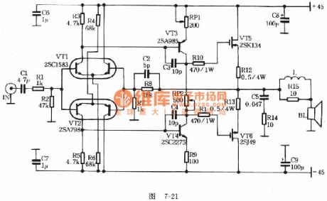
Resistor uses the1/2W high quality metal film resistor. The capacitor uses the imported CBB capacitor. All the transistors must be matched strictly. Matching error must be controlled in 3%. L uses the 1.0mm enameled wire with 10 turns tightly wound on 12mm frame. You can adjust the quiescent currentaround 100mA afterpower amplifier tube welding correctly andcheck the matching transistor error if midpoint potential of the circuit can not be controlled under 30mV.
(View)
View full Circuit Diagram | Comments | Reading(4900)
AT-HA2002 Headphone amplifier copy diagram
Published:2011/8/9 2:25:00 Author:Rebekka | Keyword: Headphone amplifier, copy diagram
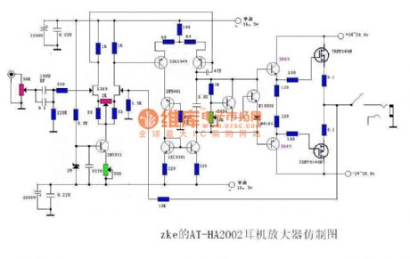
AT-HA2002 Headphone amplifier copy diagram is shown as below.
(View)
View full Circuit Diagram | Comments | Reading(1998)
6P6P Headphone amplifier circuit diagram
Published:2011/8/11 2:18:00 Author:Rebekka | Keyword: Headphone amplifier
View full Circuit Diagram | Comments | Reading(596)
Automatic cycle timer circuit diagram
Published:2011/8/11 2:42:00 Author:Rebekka | Keyword: Automatic cycle timer

Automatic cycle timer circuit diagram is shown as above. It is composed of pulse oscillator, time base circuit composed of multi-level divider, double-contact state trigger, the relay, driver circuit and the power supply etc. (View)
View full Circuit Diagram | Comments | Reading(1548)
High-precision adjustable digital timer circuit diagram
Published:2011/8/11 2:42:00 Author:Rebekka | Keyword: High-precision, adjustable digital timer


The high precision quartz crystal oscillator is composed of the CD4060 and the 32768 Hz ac quartz crystal. It passes the internal multi-stage and separates frequency output a precise second source. It can form a high precision adjustable digital timer by peripherals multi-stage separate frequency band. It can provide accurate time signal for some instruments, and it can also be used for the precise timing control of equipment. Its componentsare shown in figure. (View)
View full Circuit Diagram | Comments | Reading(1912)
High-precision time delay timing controller circuit diagram
Published:2011/8/11 2:40:00 Author:Rebekka | Keyword: High-precision , time delay, timing controller

The low frequency RC roscillato oscillator is composed of CD4060 oscillator. It can output a long time base signal after passing the internal frequency division. When the long-time time base signal is divided by multi-level frequency again, a longer time delay time can be gotten, thenit form a high-precision time delay timing controller . The constitution circuit is shown as above. (View)
View full Circuit Diagram | Comments | Reading(992)
Precision adjustable timer(CD4017) circuit diagram
Published:2011/8/11 2:39:00 Author:Rebekka | Keyword: Precision adjustable timer

Precision adjustable timer(CD4017) circuit diagram is shown as above.
It uses crystal oscillator composed of CD4060 and quartz crystal to generate base signal. It is an adjustable timer using multi-level digital frequency circuit to make frequency division. (View)
View full Circuit Diagram | Comments | Reading(2389)
The differential input and differential output amplifying circuit composed of the INA102
Published:2011/8/11 2:37:00 Author:Rebekka | Keyword: differential input , differential output , amplifying circuit

The figure shows the differential input differential output amplification circuit. In some applications, the signal source and the output voltage are not allowed to grounding, at this time, it should use the differential input and output, this circuit differential way can be composed by the INA102 and INA105. The figure shows the circuit comosed of the INA102, andthis kind of amplifier circuit does not need external components. Each INA102 voltage magnification factor is l00, ifit has different phase (voltage amplifier magnification factoris negative and positive), the general voltage amplifier magnification factor is 200. The total output voltage Vo = 200 Vi. (View)
View full Circuit Diagram | Comments | Reading(721)
Broadband differential input / differential output amplifier circuit diagram composed of OPA606
Published:2011/8/11 2:29:00 Author:Rebekka | Keyword: Broadband , differential input, differential output , amplifier

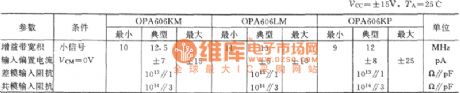
When the input / output signals are not allowed to ground and they need a wide pass band, the icon broadband differential input / differential output amplifier can be used. In the figure, the circuit uses two types of broadband FET input operational amplifiers OPA606. The device uses the dielectric isolation process, so the op amp is used as Difet op amp. The device has a high input impedance and low input bias current, in addition, OPA606 op amp circuit uses laser trimming technology, thus OPA606 has the features of low offset voltage and low noise.
(View)
View full Circuit Diagram | Comments | Reading(1385)
The differential amplifier with low-pass filtering circuit composed of the OPA2604
Published:2011/8/11 2:31:00 Author:Rebekka | Keyword: differential amplifier , low-pass filtering
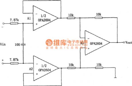
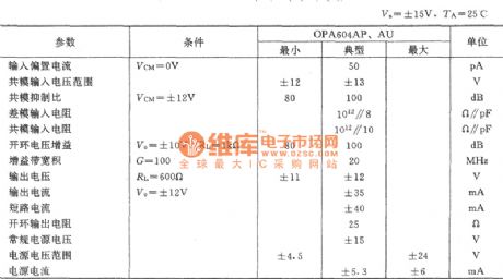
The figure shows a low pass filtering differential amplifier circuit. This circuit has the 100 Hz ac low pass filtering, differential input, single-end outputand high fidelity. The OPA2604 amplifier circuit is the mosfet inputdual op-amp integrated circuit. The OPA2604 is connected into two voltage follower. It is shown in figure A1, A2. Because OPA2604 has a very high input impedance (1012 Ω / / 8 pF) and a very low offset current (50 pA), therefore it can ensure the circuit has good filtering effect. The OPA604 is single op-amp and OPA2604 is double op-amp. Both characteristics are completely the same.
(View)
View full Circuit Diagram | Comments | Reading(1652)
LM3886 Subwoofer circuit diagram
Published:2011/8/9 2:24:00 Author:Rebekka | Keyword: Subwoofer

View full Circuit Diagram | Comments | Reading(4016)
| Pages:553/2234 At 20541542543544545546547548549550551552553554555556557558559560Under 20 |
Circuit Categories
power supply circuit
Amplifier Circuit
Basic Circuit
LED and Light Circuit
Sensor Circuit
Signal Processing
Electrical Equipment Circuit
Control Circuit
Remote Control Circuit
A/D-D/A Converter Circuit
Audio Circuit
Measuring and Test Circuit
Communication Circuit
Computer-Related Circuit
555 Circuit
Automotive Circuit
Repairing Circuit