
Circuit Diagram
Index 546
AN3311S camera video magnetic read head replay integrated circuit
Published:2011/8/11 20:17:00 Author:TaoXi | Keyword: camera video, magnetic read head, replay integrated circuit


The AN3311S is designed as the camera video magnetic read head replay integrated circuit which is produced by the Panasonic company that can be used in the Panasonic series camera.
The AN3311S integrated circuit has the 4 magnetic read head preamplifier, the magnetic read head switching switch, the envelope comparator, the peak value amplification circuit, the color changing amplification circuit, the AGC amplification circuit. The internal circuit block diagram and the typical application circuit is as shown in figure 1-14, the pin functions and data is as shown in table 1-13.
Table 1-13 The pin functions and data
(View)
View full Circuit Diagram | Comments | Reading(675)
Electric fan infrared remote control device
Published:2011/8/11 20:10:00 Author:TaoXi | Keyword: Electric fan, infrared, remote control device

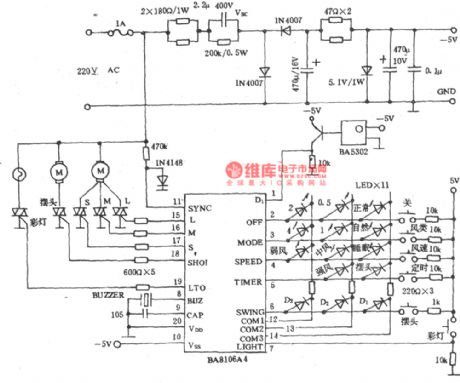
Emitter:
Receiver:
(View)
View full Circuit Diagram | Comments | Reading(1076)
Incubator constant temperature control circuit
Published:2011/8/14 19:20:00 Author:TaoXi | Keyword: Incubator, constant temperature, control circuit

The incubator constant temperature control circuit is as shown in the figure. In this circuit, the control voltage has the linear relationship with the effective value of the heater converter, in the positive half cycle of the control thyristor vs cathode voltage, the AC22V voltage charges the timing capacitor C3 through the VD1 and R2. A4 is the comparator, it compares the voltage of C3 with the heater control voltage of C2, when the voltage of C3 is the same as the voltage of C2, A4 supplies the trigger pulse to the vs gate pole. This circuit uses the U2 to control the V2's pulse position, and it makes the C3 reset through VT5. The S shape U3 waveform makes the U2 have the good linear relationship with the effective value of the heater converter.
(View)
View full Circuit Diagram | Comments | Reading(2359)
The regulator: DC-DC circuit, power supply monitor pin and its main features AN8000M
Published:2011/8/23 23:44:00 Author:Seven | Keyword: DC-DC circuit, power supply, monitor pin
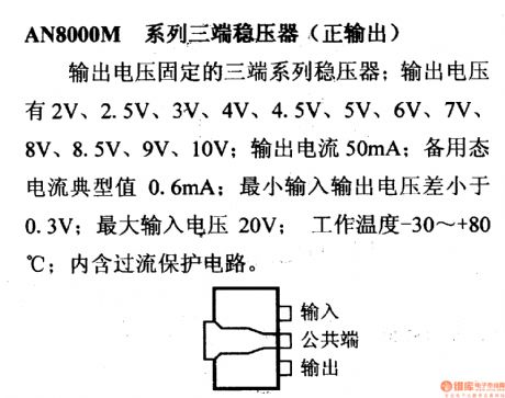
The 3-terminal stabilizer (forward output) of AN8000M series This is a 3-terminal stabilizer with a fixed output voltage; the output voltage can be 2V, 2.5V, 3V,4V, 4.5V, 5V, 6V, 7V, 8V, 9V and 10V; the output current 50mA; the typical value of the standby state current is 0.6mA; the minimum input-output voltage difference is lower than 0.3V; the max input voltage is 20V; the working temperature is -30~+80⁰C; it contains the over-current protection circuit.
(View)
View full Circuit Diagram | Comments | Reading(505)
The regulator: DC-DC circuit, power supply monitor pin and its main features LM138/238/338
Published:2011/8/23 22:23:00 Author:Seven | Keyword: DC-DC circuit, power supply, monitor pin

LM138/238/338--the adjustable 3-terminal stabilizer (forward output)This is a 3-terminal stabilizer with adjustable output voltage; its output voltage range is 1.2~32V; its maximum output current is 5A; its input stabilization typical value is 0.005%; its max input-output voltage difference is 35V; it contains the secure working area protection and overheat protection and current limitation circuit.
(View)
View full Circuit Diagram | Comments | Reading(750)
The regulator: DC-DC circuit, power supply monitor pin and its main features LM137/237/337
Published:2011/8/23 22:23:00 Author:Seven | Keyword: DC-DC circuit, power supply, monitor pin

LM137/237/337--the adjustable 3-terminal stabilizer (output)
(View)
View full Circuit Diagram | Comments | Reading(847)
The regulator: DC-DC circuit, power supply monitor pin and its main features CW117M/217M/317M
Published:2011/8/24 0:36:00 Author:Seven | Keyword: DC-DC circuit, power supply, monitor pin
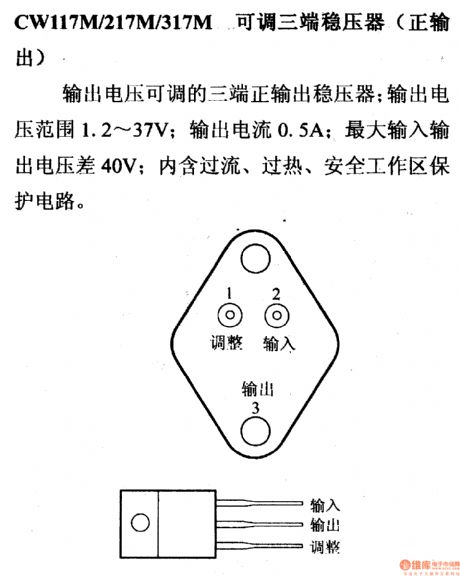
CW117M/217M/317M--the adjustable 3-terminal stabilizer (positive output)This is an adjustable 3-terminal stabilizer whose output voltage is adjustable; the output voltage range is 1.2~37V; the output current is 0.5A; the max input-output voltage difference is 40V; it contains the over-current, over-heat and secure working area protection circuit.
(View)
View full Circuit Diagram | Comments | Reading(585)
The regulator: DC-DC circuit, power supply monitor pin and its main features CW117L/217L/317L
Published:2011/8/24 0:37:00 Author:Seven | Keyword: DC-DC circuit, power supply, monitor pin
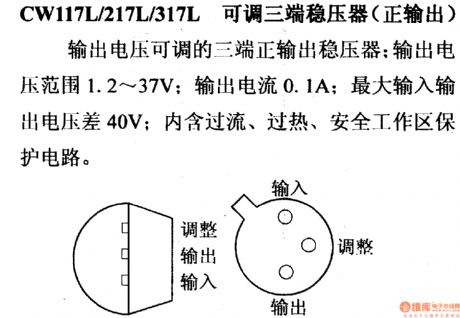
CW117L/217L/317L--the adjustable 3-terminal stabilizer (positive output) This is an adjustable 3-terminal stabilizer whose output voltage is adjustable; the output voltage range is 1.2~37V; the output current is 0.1A; the max input-output voltage difference is 40V; it contains the over-current, over-heat and secure working area protection circuit.
(View)
View full Circuit Diagram | Comments | Reading(576)
The regulator: DC-DC circuit, power supply monitor pin and its main features BA6121
Published:2011/8/24 0:15:00 Author:Seven | Keyword: DC-DC circuit, power supply, monitor pin
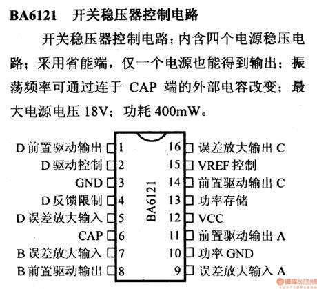
The switch stabilizer control circuit of BA6121This is a switch stabilizer control circuit which contains 4 power supply stabilizer circuits. It is adopted with the energy-saving terminals, by which even only one power supply can generate output; the oscillating frequency can be changed by the external capacitor linking to CAP terminal; the max power supply voltage is 18V; the power consumption is 400mW.
(View)
View full Circuit Diagram | Comments | Reading(606)
78PGA--The regulator: DC-DC circuit, power supply monitor pin and its main features
Published:2011/8/23 22:21:00 Author:Seven | Keyword: DC-DC circuit, power supply, monitor pin
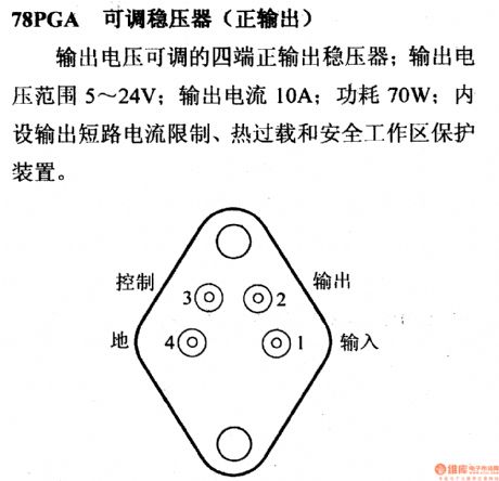
78PGA adjustable stabilizer (positive output) This is a 4-terminal positive stabilizer whose output voltage is adjustable; its output voltage range is 5~24V; its output current is 10A; its power consumption 70W; it contains the output short circuit current limitation, heat over-load and secure working area protection device.
(View)
View full Circuit Diagram | Comments | Reading(576)
The regulator: DC-DC circuit, power supply monitor pin and its main features AN6530/6531
Published:2011/8/23 22:22:00 Author:Seven | Keyword: DC-DC circuit, power supply, monitor pin
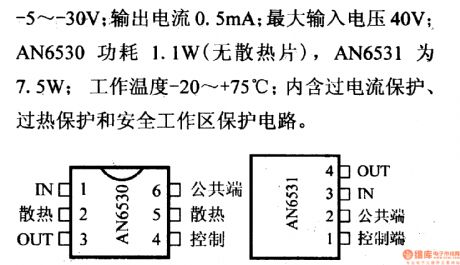
AN6530/6531 the adjustable regulator (forward output) This is a 4-terminal stabilizer whose output voltage is stable; the output voltage range is -5~-30V; output current is 0.5mA; the maximum input voltage is 40V; AN6530 power consumption is 1.1W (without radiators); it contains over-current protection, over-heat protection and secure working area protection circuit. (View)
View full Circuit Diagram | Comments | Reading(517)
The regulator: DC-DC circuit, power supply monitor pin and its main features AN5902S
Published:2011/8/23 22:21:00 Author:Seven | Keyword: DC-DC circuit, power supply, monitor pin
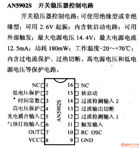
AN5902S--the switch stabilizer control circuit This is a switch stabilizer control circuit; either the insulated or non-insulated can be used; it can be oscillated with a 2.6V voltage; it contains the soft starting circuit;it can be triggered externally; the max power supply voltage is 14.4V; the max power supply current is 12.5mA; the working temperature is -20~+70⁰C; it contains the over-voltage, over-current, high power supply voltage, low power supply voltage and other protection circuits.
(View)
View full Circuit Diagram | Comments | Reading(486)
The regulator: DC-DC circuit, power supply monitor pin and its main features AD580
Published:2011/8/23 22:21:00 Author:Seven | Keyword: DC-DC circuit, power supply, monitor pin

AD580 reference voltage circuit (+2.5V) This is a wide band 3-terminal Vref circuit; its output voltage is 2.5V; the primary fault of AD580M output voltage is ±4%; the temperature drift of AD580U is lower than 10*10-6/⁰C; the long-term stability is 250μV; the input voltage range is 4.5~30V; the max input voltage is 40V; when the environment temperature is lower than 25⁰C, the power consumption is 350mW.
(View)
View full Circuit Diagram | Comments | Reading(905)
The regulator: DC-DC circuit, power supply monitor pin and its main features 79N00
Published:2011/8/23 22:21:00 Author:Seven | Keyword: DC-DC circuit, power supply, monitor pin

The 3-terminal stabilizer (negative output) of 79N00 series This is a 3-terminal positive stabilizer with fixed output voltage; its max output current 300mA; the max input voltage of 79N04~79N18 IS -35v; the max input voltage of 79N20 and 79N24 is -40V; the power consumption is 8W; its working temperature is -29~+80⁰C; it contains the over-current limitation, over-heat protection and secure working area limitation circuit. The types of similar products are AN79N00 and μPC79N00H.
(View)
View full Circuit Diagram | Comments | Reading(662)
The main features of the amplifier pin signal--μA702 wide frequency band general computer
Published:2011/8/23 22:48:00 Author:Seven | Keyword: main features, pin signal, wide frequency band, general computer
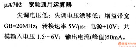
μA702 wide frequency band general computer Low maladjustment voltage; low maladjustment voltage drift; the band width of the gain is GB=20MHz; converting speed rate is 5V/μs; power supply is ±10V; common mode input voltage is 1.5V~6V; output current (peak value) is 50mA.
(View)
View full Circuit Diagram | Comments | Reading(753)
The main features of the amplifier pin signal--μA715 high computing amplifier
Published:2011/8/23 22:17:00 Author:Seven | Keyword: main features, high computing amplifier, pin signal
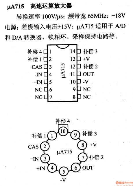
μA715 high computing amplifier Converting speed rate is 100V/μs; frequency band width is 65±MHz; ±18V power supply; difference mode input voltage is ±15V; μA715 is suitable for A/D and D/A converter, PLL, sampling maintenance circuit and so on.
(View)
View full Circuit Diagram | Comments | Reading(620)
The main features of the amplifier pin signal--μA739/749 dual low-noise computing amplifier
Published:2011/8/23 22:17:00 Author:Seven | Keyword: main features, pin signal, computing amplifier
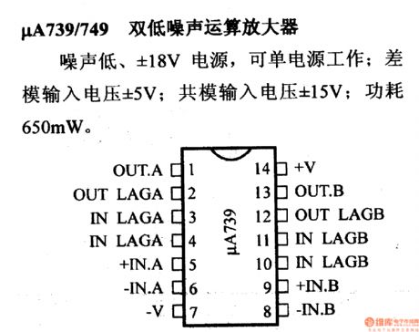
μA739/749 dual low-noise computing amplifier
Low noise, ±08V power supply, single power supply available; difference mode input voltage is ±5V; common mode input voltage is ±15V; power consumption is 650mA.
(View)
View full Circuit Diagram | Comments | Reading(1001)
The main features of the amplifier pin signal--μA771 general JFET input computing amplifier
Published:2011/8/23 22:18:00 Author:Seven | Keyword: main features, amplifier, JFET
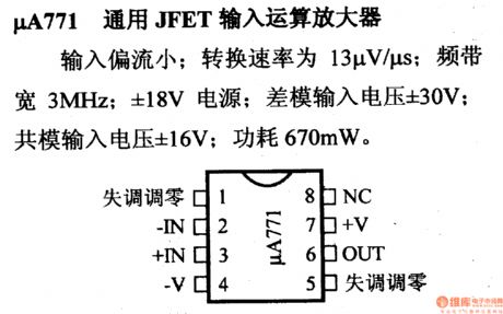
μA771 general JFET input computing amplifier Low input bias current; converting speed rate is 13μV/μs; frequency band width is 3MHz; ±18V power supply; difference mode input voltage is ±30V; common mode input voltage is ±16V; power consumption is 670mA.
(View)
View full Circuit Diagram | Comments | Reading(695)
The main features of the amplifier pin signal--μA772 dual general JFET input computing amplifier
Published:2011/8/23 22:18:00 Author:Seven | Keyword: main features, pin signal, JFET, input computing amplifier
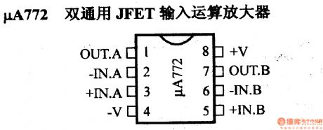
μA772 dual general JFET input computing amplifier
(View)
View full Circuit Diagram | Comments | Reading(698)
The main features of the amplifier pin signal--μA774 quadruple general JFET input computing amplifier
Published:2011/8/23 22:18:00 Author:Seven | Keyword: main features, pin signal, computing amplifier, JFET
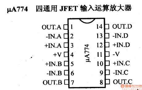
μA774 quadruple general JFET input computing amplifier
(View)
View full Circuit Diagram | Comments | Reading(652)
| Pages:546/2234 At 20541542543544545546547548549550551552553554555556557558559560Under 20 |
Circuit Categories
power supply circuit
Amplifier Circuit
Basic Circuit
LED and Light Circuit
Sensor Circuit
Signal Processing
Electrical Equipment Circuit
Control Circuit
Remote Control Circuit
A/D-D/A Converter Circuit
Audio Circuit
Measuring and Test Circuit
Communication Circuit
Computer-Related Circuit
555 Circuit
Automotive Circuit
Repairing Circuit