
Circuit Diagram
Index 555
Mellow sound pure class A power amplifier circuit diagram
Published:2011/8/9 2:23:00 Author:Rebekka | Keyword: Mellow sound, pure class PA, power amplifier
View full Circuit Diagram | Comments | Reading(5007)
Distance isolation temperature analog circuit diagram
Published:2011/8/16 2:52:00 Author:Rebekka | Keyword: Distance isolation , temperature analog


The figure shows the temperature analog circuit over long distances. In the practical application of the power system, the temperature of the equipment must be sent to the distance monitoring center, and it matchs with the measurement circuit, whichis isolated from the high voltage.In thecircuit, RTD is the platinum resistance temperature sensor, when the temperature rises, RTD resistance will be increased. The XTR101 has a high precision and WenPiao advantages, it can turn the temperature conversion into current signal, and it is easy to be transmitted over a long distance, because voltage signal in long-distance transmission loss error is large and vulnerable to electromagnetic interference.
(View)
View full Circuit Diagram | Comments | Reading(885)
1 ~ 5 V / 4 ~ 20 mA isolation converter circuit composed of the 3656 isolated amplifier
Published:2011/8/16 2:31:00 Author:Rebekka | Keyword: isolated amplifier , isolation converter


In the industrial real-time control system, in order to realize the long distance transmission signal, itoften needs to standard voltage signal 1 ~ 5 V switching for standard 4 to 20 mA current signal, because transmission current signal transmission loss is small, the low electromagnetic interference is low, it is also easy to identify, power lost or failure of open. Here 4 mA means zero level, 20 mA means the maximum signal. The figure shows the 1 ~ 5 V / 4 ~ 20 mA isolation converter composed of the 3656 isolated amplifier. Figure (b)shows 3656 internal structure.
(View)
View full Circuit Diagram | Comments | Reading(798)
The resistance strain guage application circuit diagram of ADT70ADT70 platinum RTD signal conditioner
Published:2011/8/16 2:23:00 Author:Rebekka | Keyword: resistance strain guage , application circuit , platinum RTD signal conditioner


The application circuit of the ADT70 resistance strain instrument is shown in figure. The measurement bridge is composed of the temperature compensation chipR1, measurement strain gaugeR2, wire wound resistors R3, R4, its value is1 k Ω. The bridge road working currrent is provided by IOUTA and IOUTB. Each bridge arm passing current is 1 mA. Whenit has noexternal force, the balance of the bridgeshould beset. When the specimens are caused by external deformation, the measured resistance strain gauge change makes the bridge out of balance, the diagonal outputs weak voltage signal △ u, the formula:
(View)
View full Circuit Diagram | Comments | Reading(612)
Any input voltage converting into 4 ~ 20mA V/ I converter circuit diagram
Published:2011/8/16 21:39:00 Author:Rebekka | Keyword: V/ I converter circuit , 4 ~ 20mA

Any input voltage converting into 4 ~ 20mA V I converter circuit composed of isolated amplifier 3656 is shown as above.3656 amplifier is an isolated amplifier whichuses a hybrid integrated circuit for signal amplifier and isolation of power supply. It has a strong processing ability of analog signal because it uses an advanced modulation techniques and small hybrid transformer. The outstanding advantages of 3656 are: High adaptability and excellent performance. The ground terminals of input circuit, output circuit and power circuit are independentto each other. And they are not connected with each other to achieve the three-port isolation. (View)
View full Circuit Diagram | Comments | Reading(882)
High-precision long-range temperature measurement circuit composed of the ISO120 and XTR101
Published:2011/8/9 1:58:00 Author:Rebekka | Keyword: High-precision long-range temperature measurement

The high-precision long-range temperature measurement circuit composed of the ISO120 and XTR101 is mainly used in remote temperature measurement, temperature measurement accuracy is high and in the strong noise of the measurements. The ISO120 is the duty factor modulation / demodulation techniques designed a novel isolation amplifier. Isolation layerhas 2 matching lpF differential capacitors, the transmission is digital signal. The digital signal transmission will not affect the signal characteristics of isolated components of integrity. It also has good high frequency transient performance. The figure shows the high-precision long-range temperature measurement circuit composed of the ISO120 and XTR101. (View)
View full Circuit Diagram | Comments | Reading(670)
LM4808 typical circuit diagram for two-channel headphone amplifier
Published:2011/8/16 21:49:00 Author:Rebekka | Keyword: two-channel headph amplifier

Figure shows the LM4808 for dual-channel amplifier typical circuit. Left and right channel audio signals are inputed LM4808 2, 6 feet respectively. After being amplified by internal amplifier, then they will be output by the foot 1, 7 respectively. The coupling capacitor Co isadded to the speaker. Amplifier gain is determined by resistors Ri and Rf, Av = Rf / Ri. The maximum power is PDMAX=VDD2/2π2RL. The LM4808 packaging has two amplifiers, so the total power consumption should be multiplied by 2.It is applied in a large temperature rangeenvironment , LM4808 does not install the heat sink. External input resistors and capacitors determine the input-3dB bandwidth: Input-3dB bandwidth fi-3db = 1/2πRiCi; Output-3dB bandwidth fo-3dB = 1/2πRLCo.
(View)
View full Circuit Diagram | Comments | Reading(2740)
The choking phenomenon and the eliminating measure of operational amplifier circuit diagram
Published:2011/8/9 1:51:00 Author:Rebekka | Keyword: choking phenomenon , the eliminating measure, operational amplifier

When the integrated operational amplifier is choking, the amplifier circuit will lose the ability to zoom. It is equivalent to the signal which is blocked by the same op amp.For example, thevoltage follower will often occur choking as the width of the input and output voltage of the followeris the same. Its input signal width is ususlly large(when the follower is the output stage). If the op amp input stage bias voltage is less than the peak input signal peak, the peak of the input stage will turn to saturated. When the saturation occurs, the input and output voltage becomes the same phase, the negative feedback becomes a positive feedback. Obviously, the positive and negative feedback will make the input stage bein the saturated mode. The input signal cannot output normally, and the choking phenomenon will occur. (View)
View full Circuit Diagram | Comments | Reading(641)
LM4910 For two-channel amplifier typical circuit diagram
Published:2011/8/16 22:18:00 Author:Rebekka | Keyword: two-channel amplifier
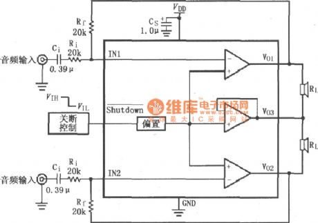
Figure shows the LM4910 for dual-channel amplifier typical circuit. Left and right channel audio signals are inputed LM4910 (MSOP / SO packaging) 1,2 feet respectively. After being amplified by internal amplifier, then they will be outputed by the foot 8, 7, 6 respectively and added to each speaker channel directly. Amplifier gain Av =- Rf / Ri, the maximum poweris PDMAX = 4VDD2/π2RL. External input resistors and capacitors determine the input-3dB bandwidth, taking Ci ≥ 1 / (2π × 20kΩ × 20Hz) with approximately 0.39μF capacitor. LM4910's pin 3 isconnect shutdown control outside.It is allowed to work when the 3 feet connect VDD (high level); It is not allowed to work when the 3 pin connect ground (low).
(View)
View full Circuit Diagram | Comments | Reading(1229)
LM4910 minimum output noise / reduce output power circuit diagram
Published:2011/8/16 22:17:00 Author:Rebekka | Keyword: minimum output noise , reduce output power

The figure shows the LM4910's minimum output noise / reduce the output power circuit. Measures to reduce the output noise are: it adds a resistor Rseries in series between the output and the load to reduce the output noise and achieve the purpose of reducing noise. The two ends of feedback resistance Rf are connected ahigh frequency bypass capacitor Cf in parallelis for keeping down high-frequency noise. J1 is a shorted jumper. The amplifier is in shutdown mode and power consumption is minimum when J1 short jumper is earthing. When J1 short jumper is off(VDD high level), the amplifier is in working mode and the power dissipation is PDMAX=4VDD2/π2RL.
(View)
View full Circuit Diagram | Comments | Reading(1183)
LM4911 Different power conduction time recommended circuit diagram
Published:2011/8/16 22:09:00 Author:Rebekka | Keyword: MOSFET, Different power , conduction time

LM4911 Different power conduction time recommended circuit diagram is shown as below. The circuit uses a controller. The MOSEFT tube of the controller controls the LM4911 shutdown control (SD) end to achieve on-time regulation of the amplifier.
(View)
View full Circuit Diagram | Comments | Reading(647)
LM4915 Single-channel pseudo differential headphone amplifier circuit diagram
Published:2011/8/16 22:08:00 Author:Rebekka | Keyword: Single-channel pseudo differential, headphone amplifier
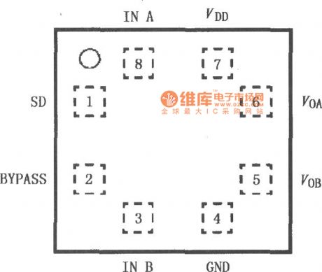
LM4915 is a pseudo-differential audio power amplifier. It is mainly used for demanding mono headset such as mobile phones and other portable audio devices. LM4915 uses 3V power supply. The average power is output 90mW and it drives 32Ω BTL load. LM4915 has a Low-power shutdown mode. Just drive control logic active low-side. LM4915 has an internal thermal shutdown protection agency. It contains a modified Cameroon - flapping sound elimination circuit. The internal fixed gain is set to 6dB. The pinout is shown as below.
(View)
View full Circuit Diagram | Comments | Reading(651)
The positive and negative values gain of adjustable amplifier circuit composed of LM107
Published:2011/8/9 2:07:00 Author:Rebekka | Keyword: positive value gain , negative value gain , adjustable amplifier


Figure (a) is the differential input switching circuit. The input end of the circuit uses a double-pole double-throw switch S to achieve positive and inverting amplification switch. It also uses four high-precision equivalent resistor R to keep the gain value. It is actually a positive and inverting voltage follower, when the S in N (ie S and the upper part of the figure the two contacts N and N 'on), the same phase follower circuit, the circuit has the following relationship: When S is placed in I and I ', the circuit has the following relationship:
(View)
View full Circuit Diagram | Comments | Reading(705)
Adjustable regulated power supply circuit diagram with 3~9V sampling ratio
Published:2011/8/9 2:03:00 Author:Rebekka | Keyword: Adjustable, regulated power supply , 3~9V , sampling ratio
View full Circuit Diagram | Comments | Reading(1167)
IOV fixed power supply circuit diagram with l20~250V grid voltage
Published:2011/8/9 2:01:00 Author:Rebekka | Keyword: Grid voltage , fixed power supply, l20~250V
View full Circuit Diagram | Comments | Reading(1300)
LM4921 for dual-channel headphone amplifier typical circuit diagram
Published:2011/8/16 22:00:00 Author:Rebekka | Keyword: dual-channel headphone amplifier
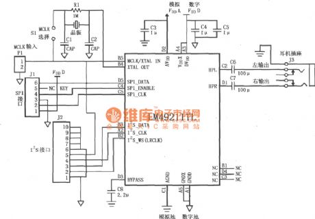
Figure shows the typical circuit of LM4921 stereo headphone amplifier. SPI interface bus J1 input controls lines signal: serial data signal SPI-DATA, serial enable signal SPI-ENABLE, serial clock signal SPI-CLK. J2 input of the I2S interface bus controls the full range of serial digital audio signal: I2S data signals I2S-DATA, I2S clock I2S-CLK. I2S word select signal I2S-WS (also known as the Right / Left Select). MCLK signal is input from P1: When S1 is off, it selects the external master clock MCLK input; when S1 is short, it uses internal oscillator (11.2896MHz).
(View)
View full Circuit Diagram | Comments | Reading(1840)
LMV1012-07/15/25 High gain microphone amplifier circuit diagram
Published:2011/8/16 22:25:00 Author:Rebekka | Keyword: High gain , microphone amplifier
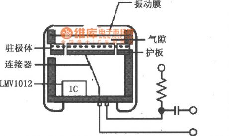
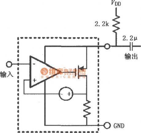
LMV1012 is a small electret microphone audio amplifier series, which is mainly used to replace the widely used JFET amplifier. LMV1012 seriesareused for adapting to the environmental site or RF noise that requires signal integrity requirements for applications, such as cellular communications systems, PDA's, car accessories etc. It guarantees 2.2 ~ 5.0V operating voltage range, the fixed gain of 7.8dB, 15.6dB and 23.8dB. Relative to the JFET amplifier, LMV1012 series amplifier has excellent gain accuracy and temperature stability. LMV1012 series can be used for two foot small electret microphone, direct pin to pin compatible JFET microphone on the market today. The device provides two 4-bump micro SMDTM package, LMV1012TP-07、LMV1012TP-15、LMV1012TP-25 pot package 1.8mm thickness, LMV1012UP-25 pot package 1.3mm thickness. It is applicable to most small electret condenser microphone.
The pinout of LMV1012 is shown as below.
Internal circuit:
(View)
View full Circuit Diagram | Comments | Reading(1925)
10W Audio power amplifier TDA2006 typical application circuit diagram
Published:2011/8/16 22:23:00 Author:Rebekka | Keyword: 10W Audio power amplifier, typical application
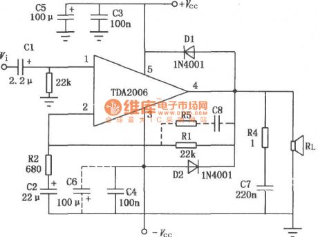
10W Audio power amplifier TDA2006's typical application circuit diagram is shown as below.
(View)
View full Circuit Diagram | Comments | Reading(5514)
20W Hi—Fi Audio power amplifier TDA2020 BTL application circuit diagram
Published:2011/8/16 22:23:00 Author:Rebekka | Keyword: 20W Hi—Fi, Audio power amplifier , BTL application

20W Hi—Fi Audio power amplifier TDA2020's BTL application circuit diagram is shown as below.
(View)
View full Circuit Diagram | Comments | Reading(3525)
Input and output in-phase addition circuit composed of CF741
Published:2011/8/16 22:22:00 Author:Rebekka | Keyword: Input and output, in-phase addition

Input and output in-phase addition circuit composed of CF741 is shown as above. In the circuit, there are many parallel connecting input signals.Its output is multiple input signals linear superposition and it does not reverse. (View)
View full Circuit Diagram | Comments | Reading(637)
| Pages:555/2234 At 20541542543544545546547548549550551552553554555556557558559560Under 20 |
Circuit Categories
power supply circuit
Amplifier Circuit
Basic Circuit
LED and Light Circuit
Sensor Circuit
Signal Processing
Electrical Equipment Circuit
Control Circuit
Remote Control Circuit
A/D-D/A Converter Circuit
Audio Circuit
Measuring and Test Circuit
Communication Circuit
Computer-Related Circuit
555 Circuit
Automotive Circuit
Repairing Circuit


