
Circuit Diagram
Index 550
The circuit diagram of using TV remote controller to cut off household appliance power supply
Published:2011/8/11 6:24:00 Author:nelly | Keyword: TV remote controller, household appliance, power supply
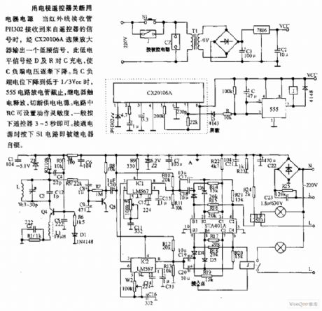
Using TV remote controller to cut off the household appliance power supply. When the infrared light-receiving diode PH302 receives the remote controller's signal, a low frequency signal is outputed by CX20106A frequency selective amplifier, this low level signal charges to C by D and R, C's negative terminal voltage drops. When it drops to lower than 1/3 VCC, the 555 circuit discharge tube is turned off, the relay is electric shocked and released, the power supply is cut off. In the circuit, RC can set action sensitivity by pressing remote controller for 3~5s. When the power supply turns on, pressing S1 circuit, then the relay is self-locking.
(View)
View full Circuit Diagram | Comments | Reading(1722)
Disyllable control citcuit diagram
Published:2011/8/11 6:06:00 Author:nelly | Keyword: disyllable, control

This cirucit executes simple on/off control function by amplifier inputing signal. when the input tone is 1800Hz, the relay is closed by two 567 decoders with self-locking function; when the input tone is 1950Hz, the relay releases. The diode is 1N4001. The relay can adopt 12V or 14V. Q1 is 2N3906, MPS6521 or 2N2222.
(View)
View full Circuit Diagram | Comments | Reading(647)
Four channels infrared remote controller circuit diagram
Published:2011/8/11 5:57:00 Author:nelly | Keyword: Four channels, infrared remote controller
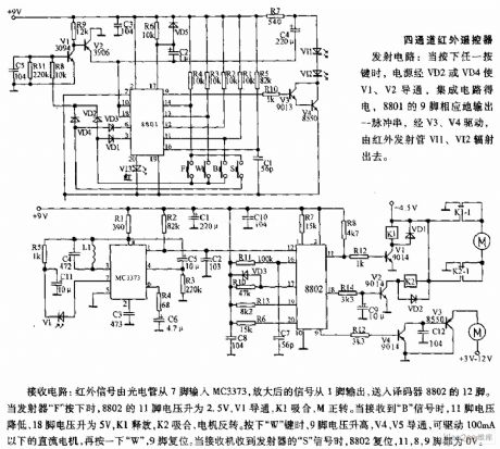
The receiving circuit: the infrared signal is inputed to MC3373 from 7 foot by phototube, the amplified signal outputs from 1 foot, it is transported into the 12 foot of decoder 8802. When the transmitter F is pressed, the voltage of 8802's 11 foot up to 2.5V, V1 turns on, K1 pulls in, M is forward rotation. When it receives B signal, 11 foot's voltage drops, 18 foot's voltage up to 5V, K1 releases, K2 pulls in, the motor is reversal rotation. Pressing W , 9 foot's voltage rises, V4, V5 turn on, it can drive the DC motors which under 100mA, pressing W again, 9 foot resets. When the receiver receives the transmitter's S signal, 8802 resets, 8, 9 feet are all 0V.
(View)
View full Circuit Diagram | Comments | Reading(1948)
Rectifier and filter circuit diagram
Published:2011/8/11 4:21:00 Author:nelly | Keyword: Rectifier, filter

The function of the rectifier and filter circuit is to change AC into 300V DC voltage. The LCD power supply circuit often adopts bridge rectifier and capacitor filter type, the typical circuit is shown in the figure.
In the circuit, VD1~VD4 are four rectifier triodes of full bridge rectifier, C is filter capacitor, the capacity is large, the value of withstand voltage should be higher than 400V, Ui is the input AC voltage, Uo is the rectified outputed DC voltage, it always is about 300V.
(View)
View full Circuit Diagram | Comments | Reading(1130)
AOC LM729 LCD switch power supply circuit diagram
Published:2011/8/11 3:41:00 Author:nelly | Keyword: LCD, switch power supply

AOC LM729 17in LCD switch power supply circuit is made as the core of control chip IC901(56*1), the circuit is shown in the figure.
(View)
View full Circuit Diagram | Comments | Reading(2906)
TEA1533 internal circuit diagram
Published:2011/8/11 5:40:00 Author:nelly | Keyword: internal circuit

The adapted commercial power grid AC voltage range of switch power supply which is composed of TEA1533 is 70~276V, on the waiting state, the power consumption is lower than 3W.
TEA1533 has complete protection circuit, it includes: demagnetization protection, over-current protection, over-voltage protection, switch transformer winding short circuit protection, under-voltage protection, chip overheat protection and the safe soft-start circuit(decreasing output power) after the protection action, according to the commercial power grid rectified voltage, it can determine the IC's start voltage. TEA1533 also has the characteristics of soft-start .
(View)
View full Circuit Diagram | Comments | Reading(2067)
The base drive circuit of white light LED
Published:2011/8/11 5:24:00 Author:nelly | Keyword: drive circuit, white light LED


Composed of switch converter, the base drive circuit of white light LED is shown in the figure1, the general switch converter controls the converter's output voltage after the feedback voltage UFB and internal reference voltage UREF are compared. If the environmental brightness signal is introduced into the LED brightness control circuit, then the white light LED drive circuit which is shown in the figure1 is changed into the circuit in the figure 2. The difference between figure1 and 2 is: the circuit in the figure 2 has Tr1, resistance R1, R2 and OP amplifier IC1.
(View)
View full Circuit Diagram | Comments | Reading(577)
Typical power supply adapter circuit diagram
Published:2011/8/11 3:37:00 Author:nelly | Keyword: power supply adapter

Most LCDs adopt external power supply adapter, the different power supply adapters have different internal circuits. As shown in the figure, it is a typical power supply adapter circuit.
(View)
View full Circuit Diagram | Comments | Reading(2949)
The VCO circuit diagram of dual D trigger
Published:2011/8/10 3:18:00 Author:nelly | Keyword: VCO, Dual D trigger

As shown in the figure, it is the VCO of dual D trigger. The circuit outputs a square wave signal with 50% duty cycle, the current consumption is low. When the input voltage is 5~12V, the output frequency range is 20~70KHz. Firstly, presuming IC-A's initial state is Q=low level. Then VD1 is cut off, C1 is charged by R1. When C1's voltage reaches the set level, IC-A is forced to reverse, the Q output terminal turns to high level, C1 is discharged by VD. At the same time, IC-A's CL input terminal turns to low level too, IC-A is forced to Q=low level.
(View)
View full Circuit Diagram | Comments | Reading(858)
Pulse shaping circuit(CD4069)diagram composed of gate circuit
Published:2011/8/10 3:39:00 Author:nelly | Keyword: Pulse, shaping circuit, gate circuit

Due to the CMOS gate circuit has a fixed threshold level, for the part of signal pulse which is lower than threshold level, the gate circuit's input terminal is no answer. With this feature, it is often directly used for the pulse's shaping. In the electronic circuits, the integrated gate circuit is one of the common used circuits. Beside used as control gate, it is also used to form the clock pulse generator. An integrated gate circuit often contains several independent gate circuits, there are alway some spare parts after constituting the circuit's main structure.
(View)
View full Circuit Diagram | Comments | Reading(1933)
Audio frequency oscillator circuit diagram with adjustable frequency composed of μA741
Published:2011/8/10 4:26:00 Author:nelly | Keyword: Audio frequency oscillator, adjustable frequency

As shown in the figure, it is the audio frequency oscillator circuit with adjustable frequency. Beside using bulb control gain, the circuit also has the automatic gain control circuit which is composed of zener diodes D1, D2 and resistance R2. With the frequency's dropping, the output amplitude will increase. When the output amplitude increases to the preset value, then the zener diode turns on. So the amplifier's gain decreases, and it can avoid the amplifier saturating. R2 is used to decrease the amplitude limit of zener diode, then it can avoid excessive distortion.
(View)
View full Circuit Diagram | Comments | Reading(1326)
AP1510 typical application circuit diagram
Published:2011/8/11 5:08:00 Author:nelly | Keyword: typical application

AP1510's 1 foot is the error feedback signal input terminal, 2 foot is output enabling terminal(high level enabling, when this foot is high level, 1 foot has output), 3 foot is oscillation set terminal(the maximum output current is set by the external resistance), 4 foot is voltage input terminal, 5, 6 feet are voltage output terminal, 7, 8 feet is groud connection. As shown in the figure, it is the AP1510 typical application circuit.
The working process of this circuit: under the control of the control circuit, the AP1510 internal switch tube is open. When the switch tube turns on, AP1510's 4 foot input voltage VIN is added to the internal switch tube S polar.
(View)
View full Circuit Diagram | Comments | Reading(849)
Voltage regulator DC-DC circuit and power supply monitor pins introduction and main features TA8002S constant voltage regulator
Published:2011/8/17 20:12:00 Author: | Keyword: Voltage regulator, power supply monitor, pins introduction, main features, constant voltage regulator
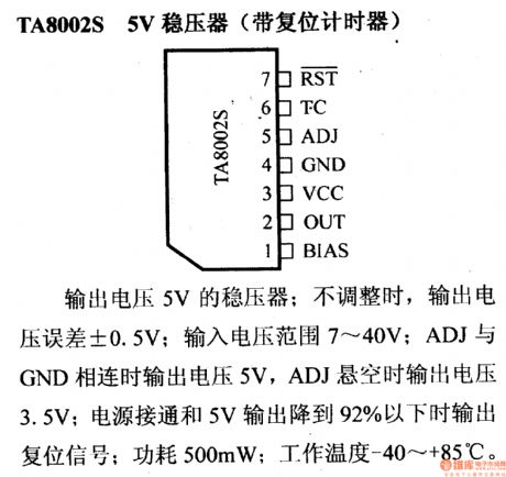
TA8002S constant voltage regulator Its output voltage is 5 V with a difference of +/- 0.5 V. And its voltage coverage is from 7 V to 40 V. When ADJ is connected to GND, its output voltage is 5 V and when ADJ is suspended in midair, the output voltage is 3.5 V. It outputs restart signal when the power supply is connected and output voltage of 5 V lowers to 92% with the power consumption of 500mW. Its operating temperature is -40oC to +85oC. (View)
View full Circuit Diagram | Comments | Reading(680)
Sine wave signal source circuit diagram with stable output
Published:2011/8/10 6:50:00 Author:nelly | Keyword: Sine wave, signal source, stable output

As shown in the figure, it is the sine wave signal source with stable output. Firstly, using the primary operational amplifier comparator, and it produces a 60Hz constant amplitude square wave. The comparator's output terminal has a pair of 6.2V zener diodes which is connected back-to-back . The next is the two-stage Sallen-key type low pass filter, it can filter all the harmonic. The capacitance coupling amplifier separates the DC component which is produced by the unequal zener voltage in the limiter circuit, then it can compensate the filter's loss, and it accurately calibrates the output amplitude to 10V peak value.
(View)
View full Circuit Diagram | Comments | Reading(881)
Voltage regulator DC-DC circuit and power supply monitor pins introduction and main features TA8001S constant voltage regulator
Published:2011/8/17 20:09:00 Author: | Keyword: Voltage regulator, power supply monitor, pins introduction, main features, constant voltage regulator

TA8001S constant voltage regulator
Its output voltage is 5 V with a difference of +/- 0.5 V. And its voltage coverage is from 7 V to 30 V. When ADJ is connected to GND, its output voltage is 5 V and when ADJ is suspended in midair, the output voltage is 3.5 V. It outputs restart signal when the power supply is connected and output voltage of 5 V lowers to 92% with the power consumption of 500mW. Its operating temperature is -40oC to +85oC. (View)
View full Circuit Diagram | Comments | Reading(761)
Voltage regulator DC-DC circuit and power supply monitor pins introduction and main features TA7900S constant voltage regulator
Published:2011/8/17 20:04:00 Author: | Keyword: Voltage regulator, power supply, main features

TA7900S constant voltage regulator
Its output voltage is 5 V with a difference of +/- 0.25 V. And its voltage coverage is from 7 V to 40 V. It outputs restart signal when the power supply is connected and output voltage of 5 V lowers to 92%. If the device makes mistake, the monitor will generate restart impulse with the power consumption of 500mW. Its operating temperature is -40oC to +85oC. (View)
View full Circuit Diagram | Comments | Reading(1294)
Voltage frequency transformation circuit diagram composed of AD654
Published:2011/8/10 6:34:00 Author:nelly | Keyword: voltage frequency, transformation

As shown in the figure, it is the low cost voltage frequency converter which is composed of AD654. Connecting the needed devices R1 and C1 as the figure, then it can be the VFC application circuit. The power voltage still can ensure the performance even drop to 4.5V, ensuring the performance to 16.5V, the maximum power consumption is 3mA(no load). The maximum frequency is 520KHz. The range of input voltage is 0~4V. The input measuring range Vi is decided by R1, Vi/R1=1mA. For example, Vi=0~1V, taking R1=1kΩ, Vi=0~5V, taking R1=5kΩ. The output frequency range is determined by C1, Fomax=1/10 C1, the frequency unit is KHz, C1's unit is μF.
(View)
View full Circuit Diagram | Comments | Reading(1428)
Voltage regulator DC-DC circuit and power supply monitor pins introduction and main features TA78L00F constant voltage regulator
Published:2011/8/17 19:40:00 Author: | Keyword: Voltage regulator, power supply monitor, main features

TA78L00F constant voltage regulator It can output fixed voltage, such as 5 V, 6 V , 8 V ,9 V, 10 V, 12 V, 15 V ,18 V, 20 V and 24 V. And its maximum output current is 150 mA. TA78L05F to TA78L15F have a maximum output voltage of 35 V, while TA78L18F to TA78L24F have a maximum input voltage of 40 V and the power consumption is 500mW. Its operating temperature is -30oC to +75oC. And it has over current and over heat protection circuit. (View)
View full Circuit Diagram | Comments | Reading(852)
SSB signal circuit diagram produced by phase-shift method
Published:2011/8/10 5:33:00 Author:nelly | Keyword: SSB signal, phase-shift method

For HAM, it is a challenge to self-made SSB transmitter, it also is a test to self-power. At present, there is little HAM can self-made SSB transmitter at home, because the crystal filter and the crystal oscillator of SSB transmitter's core parts (such as the 8998, 5KHz, 9001, used in 9MHz crystal filter, 5KHz crystal oscillator)are hard to buy, in this case, it can adopt phase-shift method to produce SSB signal, compare to the common filter method, the phase-shift method is not so better to inhibit the uselessness side band.
(View)
View full Circuit Diagram | Comments | Reading(2406)
Low frequency Wien bridge sine wave oscillator(MC1456、μA741)circuit diagram
Published:2011/8/10 4:59:00 Author:nelly | Keyword: Wien bridge, sine wave, oscillator

As shown in the figure, it is the low frequency Wien bridge sine wave oscillator circuit. This circuit adopts diode's index-number characteristic to stabilize the amplitude of 0.001Hz sine wave generator, then it has not large time constant, because the diode can quickly change their equivalent dynamic resistance. This stable circuit is similar to the limiter. The 47KΩ resistance which is in series with diode is used to decrease the diode's amplitude limit, and it can prevent circuit distortion. In general Wien bridge oscillator, due to the influence of operational amplifier's limited input impedance.
(View)
View full Circuit Diagram | Comments | Reading(3185)
| Pages:550/2234 At 20541542543544545546547548549550551552553554555556557558559560Under 20 |
Circuit Categories
power supply circuit
Amplifier Circuit
Basic Circuit
LED and Light Circuit
Sensor Circuit
Signal Processing
Electrical Equipment Circuit
Control Circuit
Remote Control Circuit
A/D-D/A Converter Circuit
Audio Circuit
Measuring and Test Circuit
Communication Circuit
Computer-Related Circuit
555 Circuit
Automotive Circuit
Repairing Circuit