


About SeekIC | Services | Payment | Advertisements service | Contact Us | Links
© 2008-2012 SeekIC.com Corp.All Rights Reserved.

Published:2011/8/14 8:43:00 Author:Christina | Keyword: Mazda, speaker circuit
The Mazda 95PROBE speaker circuit is as shown in the figure:
(View)
View full Circuit Diagram | Comments | Reading(582)
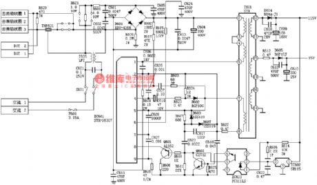
Published:2011/8/11 5:50:00 Author:Sue | Keyword: Power Supply
View full Circuit Diagram | Comments | Reading(1986)
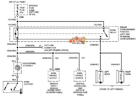
Published:2011/8/14 8:44:00 Author:Christina | Keyword: Mazda, electric seat
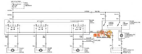
The Mazda 95PROBE electric seat circuit is as shown in the figure:
(View)
View full Circuit Diagram | Comments | Reading(517)
Published:2011/8/14 8:45:00 Author:Christina | Keyword: Mazda, alarm system circuit
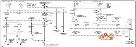
The Mazda 95PROBE alarm system circuit is as shown in the figure:
(View)
View full Circuit Diagram | Comments | Reading(507)
Published:2011/8/14 8:46:00 Author:Christina | Keyword: Mazda, demisting precipitator
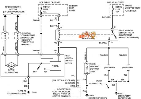
The Mazda 95PROBE demisting precipitator circuit is as shown in the figure:
(View)
View full Circuit Diagram | Comments | Reading(487)
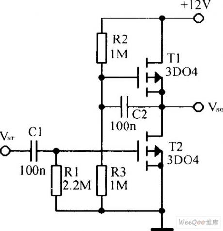
Published:2011/8/23 22:25:00 Author: | Keyword: Half wave mode, synchronous, wave-detection

The Half wave mode synchronous wave-detection circuit is as shown in the figure. This is the basic mode of the synchronous wave-detection, the output voltage U=Umcosφ, and we can get the signal amplitude of Um and phase position φ. The A1 is the buffer amplifier, the output impedance is very low. C1 is the stopping condenser, it can prevent the imbalance of A1 or the drifting to affect the performance of the circuit. A2 is the zero-cross comparator, it need to use the fast conversion speed op amp, or there will be the phase delay. The switching circuit is composed of the VT1 and VT2. The transformer T1 can make the switching signal in the floating ground state. The R1 can be used to adjust the amplitude of the switch driving signal.
(View)
View full Circuit Diagram | Comments | Reading(709)
Published:2011/8/23 22:26:00 Author: | Keyword: Switching type, voltage transform, integrated circuit


The ADP300OXX is designed as the new micro power consumption type DC/DC converter that is produced by the ANALOG DEVICES company, and it can be used in the carrier communication equipments and the bus power supply equipments.
1.Features
The ADP300OXX is the series product, the non-suffix output voltage can be adjusted, the output voltage of the ADP300OXX-3.3 is 3.3V, the output voltage of the ADP300OXX-5 is 5V, the output voltage of the ADP300OXX-l2 is 12V. And this device can be used in the voltage step-up or step-down application. The typical conversion efficiency is 80%, the switching frequency is 400kHz, and it also has the low voltage detection circuit. The internal circuit block diagram of the ADP300OXX series is as shown in the figure.
2.Pin functions and data
The ADP300OXX series IC uses the DIP-8 or SOIC-8 package, the pin functions and data are as shown in the table 1.
3.Typical application circuit
(View)
View full Circuit Diagram | Comments | Reading(595)
Published:2011/8/23 22:26:00 Author: | Keyword: synchronous, wave-detection

The synchronous wave-detection circuit composed of the MCI496L is as shown in the figure. The MCI496L is the differential circuit that is composed of the geminate transistor, the output uses the collector electrode open-circuit mode, you need to add the load resistor with it if you want to use it. The 3-time gain level shift circuit is composed of A1, the RP2 can be used to adjust the offset voltage to ensure the differential balance.
When the input signal is larger than 300mV, the internal differential amplifier of MCI496L will be in the saturated state, so at the signal input Vi port and the benchmark phase input UREF port, the attenuation network is composed of the R1, R2 and R3. So the input signal of the MCI496L can be a few volts.
(View)
View full Circuit Diagram | Comments | Reading(639)
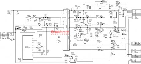
Published:2011/8/11 5:51:00 Author:Sue | Keyword: Power Supply
View full Circuit Diagram | Comments | Reading(1845)
Published:2011/8/11 5:49:00 Author:Sue | Keyword: Power Supply
View full Circuit Diagram | Comments | Reading(1928)
Published:2011/8/23 22:26:00 Author: | Keyword: Broadband level, wave-detection

The broadband level wave-detection circuit is as shown in the figure. This circuit is the broadband amplifier that is composed of the transistor, and you can connect the rectifier diode with the negative feedback loop to form the 1OMHZ, good linearity level detection circuit. In this circuit, the VT1~VT3 use the high cut-off frequency T transistor, and these transistors can form the directly coupled type amplifier circuit; the full wave rectifier circuit is composed of the diodes VD1 and VD2; the resistances R1 and R2 have the feedback function, the A1 has the differential/single polarity conversion function.
(View)
View full Circuit Diagram | Comments | Reading(678)
Published:2011/8/23 22:27:00 Author: | Keyword: double operation, amplifier, integrated circuit


The AD827AQ and AD827JN are designed as one kind of double operation amplifier integrated circuit that is produced by the MD company, and it can be used in the sound equipment, the electrical equipment and the industrial automatic control electronic circuit.
The AD827AQ and AD827JN are in the dual-row DIP package, the package has two kinds: the ceramic package and the plastic package, if the suffix is AQ, it is the ceramic package, if the suffix is JN, it is the plastic package. They have the same internal structure, they are composed of two high precision operation amplifier circuits. The pin functions and data are as shown in table 1.
The AD6524 frequency synthesizer integrated circuit
The AD6524 frequency synthesizer integrated circuit can be used in all kinds of cellphones such as the TCL2188.etc.
(View)
View full Circuit Diagram | Comments | Reading(965)
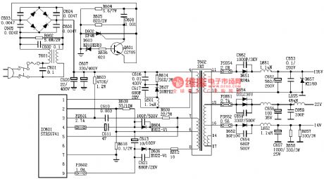
Published:2011/8/11 5:46:00 Author:Sue | Keyword: Power Supply
View full Circuit Diagram | Comments | Reading(1580)
Published:2011/8/11 5:48:00 Author:Sue | Keyword: Power Supply
View full Circuit Diagram | Comments | Reading(4690)
Published:2011/8/11 5:46:00 Author:Sue | Keyword: Power Supply
View full Circuit Diagram | Comments | Reading(1667)
Published:2011/8/11 5:44:00 Author:Sue | Keyword: Power Supply
View full Circuit Diagram | Comments | Reading(1387)
Published:2011/8/23 22:27:00 Author: | Keyword: Simple, pulse width, modulation

The simple pulse width modulation circuit is as shown in the figure. It uses the operational amplifier to form the multivibrator, so we can get the positive and negative symmetrical oscillation output signal with the duty ratio of 50%. If we change the threshold voltage from external, we can realize the pulse width modulation. If this circuit is not connected with the resistor R1, the oscillation frequency f0 is decided by the cycle of the hysteresis voltage, f0=1/2R4C1ln(1+(2R2/R3)).
If [1+(2R2/R3)]=2.718, the f0=l/(2R4C1), so we can change the duty ratio by using the external voltage to move the ±UTH through R1.
(View)
View full Circuit Diagram | Comments | Reading(2335)
Published:2011/8/11 5:43:00 Author:Sue | Keyword: Power Supply
View full Circuit Diagram | Comments | Reading(1172)
Published:2011/8/11 5:41:00 Author:Sue | Keyword: Power Supply
View full Circuit Diagram | Comments | Reading(999)
Published:2011/7/18 0:18:00 Author:Sue | Keyword: Improved, High Gain, Amplifier
The picture shows the improved high gain amplifier circuit. (View)
View full Circuit Diagram | Comments | Reading(684)
| Pages:542/2234 At 20541542543544545546547548549550551552553554555556557558559560Under 20 |
Response in 12 hours
© 2008-2012 SeekIC.com Corp.All Rights Reserved.