
Circuit Diagram
Index 559
The 4.5V charge battery power supply applicational circuit
Published:2011/8/11 21:29:00 Author:Borg | Keyword: charge battery, power supply, applicational circuit

The 4.5V charge battery power supply applicational circuit is shown in the figure.
(View)
View full Circuit Diagram | Comments | Reading(875)
Grid Electrode Drivng Circuit Composed Of M57918L
Published:2011/8/17 0:30:00 Author: | Keyword: Grid, Electrode, Drivng
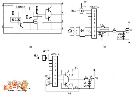
The picture shows the the grid electrode driving circuit composed of M57918L. The picture (a) is the M57918L internal equivalent circuit. The picture (b) shows the circuit driving the low-power MOSFET. In the circuit the C1 and C2's capacity is more than 200 times than Ciss (the input capacitanc of the MOSFET). If using the electrolytic capacitor, it needs to add the film capacitor in parallel with electrolytic capacitor and the film capacitor should have good high-frequency features. Its capacity is 1/200 of the C1 or C2's capacitor. The lower of the RG, the higher the switching speed would be, but it shouldn't be lower than its lower limit. The VS1 and VS2 need the regulator diode about 18V. The picture (c) is the circuit which is driving the large-power MOSFET. (View)
View full Circuit Diagram | Comments | Reading(1100)
The amplifier exposer circuit
Published:2011/8/15 21:47:00 Author: | Keyword: amplifier, exposer

The amplifier exposer circuit The circuit is a basic LDR bridge circuit, VR1 is the loading resistor of LDR. When testing, the high input impedance computing buffers IC1A and IC1B can make sure that the connection of LDR and VR1 has no effect. IC1C is the voltage comparator, which can control the brightness of the red and yellow LED. When it is at the zero point, the LED will change into red from yellow, or change from yellow into red, so it can provide with continuous illumination for VR1 and VR2. When the voltage of the cell drops to 6V, the yellow LED will indicate that the power is low.
(View)
View full Circuit Diagram | Comments | Reading(800)
Grid Electrode Driving Circuit Composed Of IR2121
Published:2011/8/17 9:45:00 Author: | Keyword: Grid, Electrode, Driving
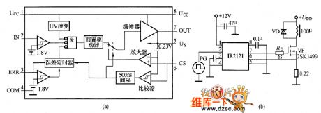
The picture shows the grid electrode driving circuit composed of IR2121. The IR2121 is a low-side grid electrode driving IC with the current-limiting function. The picture (a) shows the IR2121 internal equivalent circuit. The IR2121 has the error output port (ERR). The circuit shut-off time is set by the ERR port with the external connected capacitor. The input (IN) signal voltage level is TTL positive logic level. The threshold voltage is 1.8V. The power detecting port (CS) threshold voltage is 230mV with internal setting 500ms interval. The delay time's typical value is 700ns from detecting the over current to the circuit shutting off. (View)
View full Circuit Diagram | Comments | Reading(3899)
Grid Electrode Driving Circuit Composed Of TK75050
Published:2011/8/17 9:46:00 Author: | Keyword: Grid, Electrode, Driving

The picture shows the grid electrode driving circuit composed of TK75050. The TK75050 has the internal functions such as current limiting, thermal breakdown protection, low voltage lockout and so on. The load capacitance is 10000pF. It is the low-side grid electrode driving IC with in or out current of ±2A. The picture (a) shows the TK75050's internal equivalent circuit. And when the internal temperature is about 150℃ the over-heat protection circuit would have action. Its input (INPUT) threshold voltage is 1.6V/1.0V which is the so-called TTL voltage level. Its working voltage Ucc is 12V and if it is under 11V the low-voltage lockout circuit would have action, if it is under 10V the circuit would be shut off. This is prevent the unstable working of the circuit when its power voltage varies slowly. (View)
View full Circuit Diagram | Comments | Reading(1020)
Low-Voltage Port (Shortly Called Low Port) Grid Electrode Driving Circuit
Published:2011/8/17 0:18:00 Author: | Keyword: Low, Voltage, Port, Grid Electrode, Driving
(View)
View full Circuit Diagram | Comments | Reading(905)
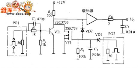
Grid Electrode Driving Circuit Composed Of Two Transistors
Published:2011/8/16 23:38:00 Author: | Keyword: Grid, Electrode, Driving, Two, Transistors
The picture shows the grid electrode driving circuit composed of VT1 and VT2 which are in the emitter follower working mode. For the power MOSFET whose drain electrode's power consumption of 100~150W, its input capacitance Ciss is thousands of pF. When the voltage UDS between drain electrode and source electrode is closing 0V, the input capacitance would increase and be more. So as the loading capacitance of the grid electrode driving circuit, the C1 is normally be 10000pF (about 0.01uF). The picture shows the grid electrode driving circuit. When the transistor VT1 is conducted it would charge the capacitor CL. When the transistor VT2 is conducted it would discharge the electricity stored by the grid electrode. The RG would limit the peak current of the charging and discharging. (View)
View full Circuit Diagram | Comments | Reading(954)
Large-Power Full Bridge Circuit
Published:2011/8/17 0:41:00 Author: | Keyword: Large, Power, Full, Bridge

The large-power circuit is always using the full-bridge circuit which is shown in the picture. In the circuit, the VF1 is N-channel power MOSFET and its output voltage is twice of the half-bridge circuit. It the load is the same, its power would be 4 times of the power of the half-bridge circuit. So it is suitable for the large-power applications.
The picture shows the large-power full-bridge circuit.
In the full-bridge circuit, the two output ports are in floating mode. So if any port is connected with the power port, it would be the short circuit mode of the load, and the elements would be damaged. So it adds the isolated transformer T1. This transformer also has the function of impedance conversion, voltage boost and buck and so on. (View)
View full Circuit Diagram | Comments | Reading(684)
Grid Electrode Basic Driving Circuit
Published:2011/8/18 3:20:00 Author: | Keyword: Grid, Electrode, Basic, Driving

The power MOSFET's grid electrode driving circuit has different kinds of types according to the differences of the switching circuit. The picture shows the single-tube and dual-tube switching circuit. The picture (a) is a basic switching circuit composed of the power MOSFET whose the source electrode is connected to the ground. Its load could be resistance, inductance, switching transformer or DC motor and so on. The picture (b) is the swithing circuit composed of two power MOSFET and the VF1 and VF2 would be connected and disconnected working at the same time. Because there are clamp diodes VD1 and VD2 connecting in the power circuit, so the power MOSFET's withstand voltage needn't have the surplus capacity. (View)
View full Circuit Diagram | Comments | Reading(628)
Narrow Pulse Driving Circuit
Published:2011/8/17 5:21:00 Author: | Keyword: Narrow, Pulse, Driving

The picture shows the circuit which could add enough reverse bias even for the narrow pulse. In the circuit shown in picture (a), when the VT1 is conducted, the current would be through R and VT3's base electrode. At the same time it would charge the capacitor C which is regarded as reverse bias power. If the VT1 is not conducted, the diode VD2 would make the VT2 conducted, the capacitor C's energy would be reversely added on the VD2's base electrode. If the carriers in VT2 are completely swept and over, it would reversely add the NSI's voltage on the VT3's base electrode through R2. For the circuit shown in picture (b), the reverse bias power C's voltage is also get from R2. The working principle is just the same with picture (a). (View)
View full Circuit Diagram | Comments | Reading(658)
The amplifier timed exposer circuit
Published:2011/8/15 21:57:00 Author: | Keyword: amplifier, timed exposer

The amplifier timed exposer can turn on the amplifier light, and the time is ranged from 1s to 20s, and it can also set the LED which flashes once per second, which is convenient for the dark room. The circuit consists of the comparator, timer and pulse timer. The comparator is used to estimate the exposing time. By adjusting VR1, the light volume on PCC1 can be tested. The timer is added on the non-inverting phase input terminal of IC1B by the VR3 adjusting Vref. When C2 is discharging, IC1B is outputting a high LEV, TR2 is conducting, the relay is working and the amplifying light is put through. (View)
View full Circuit Diagram | Comments | Reading(624)
The reporting timing contact printer circuit
Published:2011/8/15 22:15:00 Author: | Keyword: contact printer
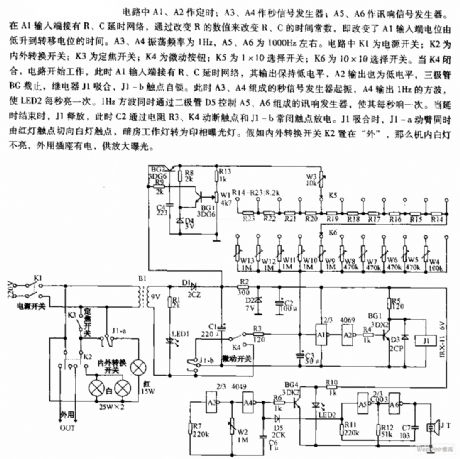
In the circuit, A1 and A2 are the timers; A3 and A4 are the second signal generators; A5 and A6 are the sound signal generator. At the input terminal of A1, the R and C time delay net is connected there, by changing the value of R, the time constants of R and C are changed, i.e the time of A1 input terminal LEV rising from low to transfer potential is changed. The oscillating frequency of A3 and A4 is 1Hz, the frequency of A5 and A6 is 1000Hz or so. In the circuit, K1 is the power supply switch; k2 is the in-out converting switch; K3 is the focus switch; K4 is the jogging switch; K6 is the 10*10 selecting switch.
(View)
View full Circuit Diagram | Comments | Reading(870)
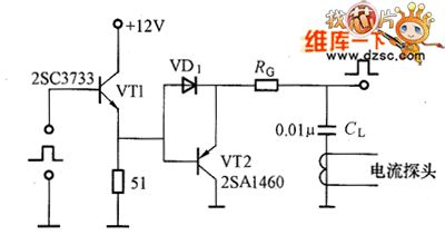
Direct Driving Circuit
Published:2011/8/13 7:35:00 Author:Robert | Keyword: Direct, Driving

The most effective method to add reverse bias voltage is using the circuit in picture (a). In this circuit when the switch transistor VT3 is disconnected, the VT2 would be conducted and add the reverse voltage to the switch transistor VT3's base electrode. Even the pulse is narrow it could add enough reverse bias voltage. But it needs the reverse bias power U2. The VT2's power is using the circuit in picture (c). It could get the voltage U2 from the transformer tapping.
The picture shows the direct driving circuit. (View)
View full Circuit Diagram | Comments | Reading(595)
Base Electrode Driving Circuit
Published:2011/8/13 7:52:00 Author:Robert | Keyword: Base Electrode, Driving

The base electrode driving circuit example is shown in the picture. When the base electrode current is big, to prevent the increasing of the storage time, it can use the Bekaa clamp circuit shown in picture (b). In the circuit, the base electrode current increases, when the transistor VT's saturation voltage is lower than UBE, the diode VD1 would be conducted. Thus it could prevent the increasing of the base electrode current. It is a circuit to prevent overexcitation.
The picture shows the base electrode driving circuit practical example.
(a)The drving circuit which the base electrode current is increasing as the ratio to the collector current.
(b)Bekaa clamp circuit. (View)
View full Circuit Diagram | Comments | Reading(700)
PWM Signal Generating Circuit
Published:2011/8/17 10:00:00 Author: | Keyword: PWM, Signal, Generating

The switching power separate excitation control method has pulse width modulation (PWM) and pulse frequency modulation (PFM). And the most cases use the PWM method. So here it would introduce the PWM control principle. The picture shows the PWM signal generating circuit diagram and working waveform. Its working process is following. By detecting the controlled voltage Uo it could get the feedback voltage Ur and then add it to the in-phase port of the amplifier A1. The fixed referenced voltage Uo is added to the out-phase port of A1. After the amplification of A1, the DC error voltage Ue is added to the out-phase port of amplifier A2. And the sawtooth signal Usa, which is generated from the fixed frequency oscillator, is added to the in-phase port of A2. (View)
View full Circuit Diagram | Comments | Reading(1027)
Regulator Power Circuit Using Luoya Improving Method
Published:2011/8/14 3:43:00 Author:Robert | Keyword: Regulator Power, Luoya, Improving, Method

The picture shows the luoya improving method circuit. The picture (a) is suitable for the 220V input, while the picture (b) is suitable for the 380V input. For example in the circuit of picture (a), if firstly make the VT1 conducted by starting the resistor R1, the transformer T1 would have excitation and add the voltage on the transformer T2 through the current-limiting resistor R3. So the VT1 would be conducted rapidly. Then is the T1 is saturated, the VT1 would disconnected and at the same time the T2 would generate the opposing electromotive force and VT2 is conducted. So the VT1 and VT2 would make the oscillation by their alternate connected and disconnected work.
(a)Suitable for 220V input. (b)Suitable for 380V input.
The picture shows the luoya improving method circuit. (View)
View full Circuit Diagram | Comments | Reading(791)
XC62AP Series Integrated Voltage Regulator Internal Diagram And Basic Application Circuit
Published:2011/8/17 10:12:00 Author: | Keyword: Integrated, Voltage, Regulator, Internal, Diagram, Basic, Application
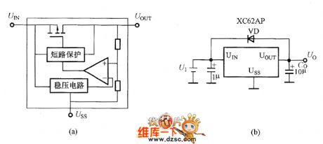
The XC62AP series integrated voltage regulator is a CMOS integrated voltage regulator with linear positive voltage output. It has output voltage of +5V (XC62AP50) and+3V (XC62AP30) and other types, which could arbitrarily set the voltage between 1.1V to 6.0V by the factory (stepped voltage is 0.1V). The XC62AP series integrated voltage regulator's internal diagram and basic application circuit is shown in the picture.
Picture (a) shows the XC62AP series integrated voltage regulator's internal diagram. Picture (b) shows the basic application circuit.
The picture shows the XC62AP series integrated voltage regulator's internal diagram and basic application circuit.
The XC62AP series integrated voltage regulator's features are super-low current consumption which typical value is 0.9uA, low voltage drop which has the typical value of 180mV at output current of 80mA, low deviation of output voltage which is about ±2%, small temperature drift. So it would be used as the super-low power consumption referenced voltage source. (View)
View full Circuit Diagram | Comments | Reading(1529)
RX5RA/RE Series Integrated Voltage Regulator Pin Configuration And Basic Application Circuit
Published:2011/8/14 5:53:00 Author:Robert | Keyword: Integrated, Voltage, Regulator, Pin, Configuration, Basic, Application
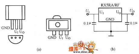
The RX5RA/RE series are three-port CMOS integrated voltage regulator with low voltage drop and low current consumption. The series have T092 and surface-mount package types. Their model names are different as their package. The T092 package is for RE5RA/RE and the surface-mount package is for RH5RA/RE. The picture shows the RX5RA/RE series integrated voltage regulator pin configuration and basic application circuit.
(a)RX5RA/RE series integrated voltage regulator pin configuration. (b)Basic application circuit.
The picture shows the RX5RA/RE series integrated voltage regulator pin configuration and basic application circuit. (View)
View full Circuit Diagram | Comments | Reading(924)
Output Voltage Adjustable Circuit
Published:2011/8/18 2:44:00 Author: | Keyword: Output, Voltage, Adjustable

The picture shows the output voltage adjustable circuit, and it also has the over-current protection circuit. The purpose of the EXT port's current limiting circuit is to protect the integrated voltage regulator. It should consider the external connecting transistor and FE's discreteness and the maximum output current, so then it could choose the R2's resistance value. For assuring the current limiting, it is connected the R3 and VT2 whose current limiting value is 0.7V/R3. The UOUT's external connected resistance RA and RB could be used to adjust the output voltage. Because the UOUT port's internal chip has connected to the high-impedance resistance (10MΩ) for detecting and the accelerated capacitance. So even the RA and RB use the hundreds KΩ resistance it would not generate the error. So this could design the low-current-consumption adjustable voltage regulator power. (View)
View full Circuit Diagram | Comments | Reading(754)
RN5RG Series Voltage Regulator Internal Diagram And Basic Application Circuit
Published:2011/8/18 2:22:00 Author: | Keyword: Voltage, Regulator, Internal, Diagram, Basic, Application

The RN5RC series is the low-voltage-drop voltage regulator with surface-mount small SOT23 package and externally connecting with a PNP transistor. The RN5RG30A (output voltage is 3V) features is following: no-load current consumption is 50pA, standby current is 0.2uA, input/output voltage difference is the transistor's conducted resistance value multiply by the output current. Its output voltage's accuracy is ±2.5%. Its output voltage's temperature feature is in ±100×10-6℃. Its input stability is 0.1%/V. It uses the SOT23 5-pin package.
The picture shows the RN5RG series voltage regulator internal diagram and basic application circuit. (View)
View full Circuit Diagram | Comments | Reading(1129)
| Pages:559/2234 At 20541542543544545546547548549550551552553554555556557558559560Under 20 |
Circuit Categories
power supply circuit
Amplifier Circuit
Basic Circuit
LED and Light Circuit
Sensor Circuit
Signal Processing
Electrical Equipment Circuit
Control Circuit
Remote Control Circuit
A/D-D/A Converter Circuit
Audio Circuit
Measuring and Test Circuit
Communication Circuit
Computer-Related Circuit
555 Circuit
Automotive Circuit
Repairing Circuit