Other Circuit
Grid Electrode Driving Circuit Composed Of Two Transistors
Published:2011/8/16 23:38:00 Author: | Keyword: Grid, Electrode, Driving, Two, Transistors | From:SeekIC
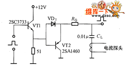
The picture shows the grid electrode driving circuit composed of VT1 and VT2 which are in the emitter follower working mode. For the power MOSFET whose drain electrode's power consumption of 100~150W, its input capacitance Ciss is thousands of pF. When the voltage UDS between drain electrode and source electrode is closing 0V, the input capacitance would increase and be more. So as the loading capacitance of the grid electrode driving circuit, the C1 is normally be 10000pF (about 0.01uF). The picture shows the grid electrode driving circuit. When the transistor VT1 is conducted it would charge the capacitor CL. When the transistor VT2 is conducted it would discharge the electricity stored by the grid electrode. The RG would limit the peak current of the charging and discharging.
Reprinted Url Of This Article:
http://www.seekic.com/circuit_diagram/Electrical_Equipment_Circuit/Other_circuit/Grid_Electrode_Driving_Circuit_Composed_Of_Two_Transistors.html
Print this Page | Comments | Reading(3)

Article Categories
power supply circuit
Amplifier Circuit
Basic Circuit
LED and Light Circuit
Sensor Circuit
Signal Processing
Electrical Equipment Circuit
Control Circuit
Remote Control Circuit
A/D-D/A Converter Circuit
Audio Circuit
Measuring and Test Circuit
Communication Circuit
Computer-Related Circuit
555 Circuit
Automotive Circuit
Repairing Circuit
Code: