
Circuit Diagram
Index 540
Grid Electrode Isolated Driving Circuit For Half-Bridge Circuit
Published:2011/8/23 23:39:00 Author:Robert | Keyword: Grid, Electrode, Isolated, Driving, Half-Bridge

The picture shows the grid electrode isolated driving circuit for half-bridge circuit. The input signal A and B are the signals provided by the switching power integrated controller. And when they are added on the transformer, the waveform's duty cycle would be below 50%. The pulse transformer T1 and T2's each winding is separated. Its primary side has two series windings. Its secondary side has two parallel windings. For reducing the VD3~VD6's positive voltage drop, it should use the schottky diode. But if it uses the general diode, that would also be OK. The driving circuit's output port is connected to the driving power MOSFET's grid electrode (G) and source electrode (S). (View)
View full Circuit Diagram | Comments | Reading(793)
four-way electronic change-over switch circuit with CD40157,CD4066
Published:2011/7/22 3:22:00 Author:chopper | Keyword: four-way, electronic, change-over switch

View full Circuit Diagram | Comments | Reading(7774)
touch type three-way audio source change-over switch circuit with CD4052,CD4011
Published:2011/7/22 3:30:00 Author:chopper | Keyword: touch type, three-way, audio source, change-over switch

View full Circuit Diagram | Comments | Reading(6347)
Grid Electrode Driving Circuit With Shortening Turn-Off Time
Published:2011/8/23 23:39:00 Author:Robert | Keyword: Grid, Electrode, Driving, Shorten, Turn-Off, Time

The picture shows the grid electrode driving circuit with shortening power MOSFET turn-off time. In the circuit shown in picture (a), the transistor VT1 and VT2 are make up the push-pull driving circuit with low output impedance. When the VF1 is conducted and the VD1 is disconnected, it would be through the grid resistance RG to charge the VF1's input capacitance Ciss. The RG limits its peak current. The VF1 turn-off time driving circuit would absorb the grid current and the diode VD1 would be conducted to short the RG. Thus the Ciss would discharge with a large current. So the electric charge stored in the grid electrode would be released rapidly.
The picture shows the grid electrode driving circuit with shortening turn-off time. (View)
View full Circuit Diagram | Comments | Reading(1122)
Push-Pull Switching Circuit With Grounding Source Electrode
Published:2011/8/23 23:39:00 Author:Robert | Keyword: Push-Pull, Switching, Grounding, Source, Electrode

In the large-power applications it usually uses the push-pull switching circuit with transformer middle tapping method. The picture shows the common-used push-pull circuit with grounding source electrode. The push-pull switching circuit's input and output's phase difference is 180°. But the switching power controller has the A phase and the B phase which also have the 180° phase difference, it could directly drive the push-pull switching circuit composed of power MOSFET. Also in no-load case the power MOSFET in the circuit would have a high voltage between its drain electrode and source electrode which would easily have breakdown. So the power MOSFET's withstand voltage must have enough surplus capacity, and also it needs the absorbing circuit to limit the surge voltage. (View)
View full Circuit Diagram | Comments | Reading(704)
Transistor Disconnecting Circuit Using Inductance Stored Energy
Published:2011/8/23 23:39:00 Author:Robert | Keyword: Transistor, Disconnecting, Inductance, Stored, Energy

The picture shows the transistor disconnecting circuit using inductance stored energy. In the circuit shown in picture (a), during the transistor VT1 conducted time, the current IL, which is through the inductance L is IL, would change to be the peak current Ip after the VT1 conducting. Ip=U1TON/Lo. When the VT1 is disconnected, for keeping the current, the reverse current Ib2, which is through the VT2 base electrode, peak current would be Ip. This would accelerate the VT1's switching time. For this kind of circuit, because the reverse current Ib2 and the transistor conducted time TON are proportional, it would not get enough reverse current when the pulse is narrow. (View)
View full Circuit Diagram | Comments | Reading(572)
touch type ten-gear interlock switch controller circuit with CD4069,CD4017
Published:2011/7/22 3:09:00 Author:chopper | Keyword: touch type, ten-gear, interlock switch, controller circuit

View full Circuit Diagram | Comments | Reading(1190)
Power Conversion Circuit Of Switching Regulator Power
Published:2011/8/23 23:40:00 Author:Robert | Keyword: Power, Conversion, Switching, Regulator

The power conversion circuit of switching regulator power has many types such as push-pull, full-bridge, half-bridge and single-ended flyback and single-ended forward and other types. The picture shows the push-pull type power conversion circuit. The control circuit would control the base electrode of the transistors VT1 and VT2. The VT1 and VT2 would be alternately connected and disconnected with PWM excitation method. Then they would convert the input DC voltage to the high-frequency square-wave AC voltage. When the VT1 is conducted, the input power voltage Ui would be through VT1 and then it is added the high-frequency transformer T1's primary winding N1. Because T1 has two main windings N1 with equal number of turns, so when the VT1 is conducted, it adds twice power voltage 2UI onto the transistor VT2 which is in disconnected mode. (View)
View full Circuit Diagram | Comments | Reading(884)
Voltage Regulator Power Luoya Method Circuit
Published:2011/8/23 23:40:00 Author:Robert | Keyword: Voltage, Regulator, Power, Luoya, Method

The picture shows the Luoya method circuit which is suitable for the 220V input. The picture (b) is suitable for 380V input. For example in the circuit shown in picture (a), the R1 is starting resistance. When the input voltage is connected, as the special difference of VT1 and VT2, if the VT1 is conducted firstly, the transformer T1 would process the field excitation and the VT1 would be conducted rapidly. If T1 is in the magnetic saturation mode, the VT1 would change to be disconnected. So the T1 would generate the opposing electromotive force which would be through the transformer's feedback winding to make VT2's base electrode get the positive bias voltage, so that it would be conducted. This repeated actions would make the transformer T1 magnetic flux have the continuous oscillation. (View)
View full Circuit Diagram | Comments | Reading(645)
Single-load multi-site switch control circuit formed by CD4017
Published:2011/7/23 2:30:00 Author:chopper | Keyword: Single-load, multi-site, switch control

View full Circuit Diagram | Comments | Reading(709)
Voltage Regulated Power Chopper Method Circuit
Published:2011/8/23 23:40:00 Author:Robert | Keyword: Voltage, Regulated, Power, Chopper, Method

1. Chopper method.The picture shows the chopper method circuit. This is a non-isolated conversion method whose conversion efficiency is beyond 85%. This method contains the buck type, boost type, and polarity inversion type.The picture (a) shows the buck type circuit. When the transistor VT1 is conducted, the U1 would be through VT1 to add onto the choke L1 and capacitance C1, thus it would provides the load power. When the VT1 is disconnected, the energy stored in L1 would be through the freewheeling diode VD1 to supply the load.The picture (b) shows the boost type circuit. When the transistor VT1 is connected, the choke L1 would store energy. (View)
View full Circuit Diagram | Comments | Reading(806)
PNP Output Regulator Grounding Current Circuit
Published:2011/8/23 23:39:00 Author:Robert | Keyword: PNP, Output, Regulator, Grounding, Current

The PNP output low-voltage-drop regulators' common weakness is the grounding current (current consumption of the regulator itself) is more than the input current. Also the output current causes the grounding current having a big variation. The PNP output regulator is that the transistor's base electrode current control the load current, thus this base electrode current would go through the ground and make up a part of the grounding current. As shown in the picture, thepicture shows the control circuit consumption current, also the picture shows the base current. The IH is output current. So, even the load current (the transistor collector electrode current) is small, the I/hFE's grounding current would also change to be the consumption current. (View)
View full Circuit Diagram | Comments | Reading(1165)
High Accuracy Constant Current Circuit
Published:2011/8/23 23:40:00 Author:Robert | Keyword: High, Accuracy, Constant, Current

The picture shows the high accuracy constant current circuit and its practical application example. In the circuit shown in picture (a), it adds the grounding loop circuit between the constant current circuit and the load. Thus the current would return to be stable rapidly when the load has changed. The A1 and VT1 make up the voltage/current conversion circuit which could convert the ground voltage signal to the +15V voltage signal needed by the constant current circuit. The A2, VT2, VT3 etc. make up the standard constant current circuit. By setting R1=R2 it could provides the equal current I1=I2. VT5's base electrode is provided the +5V stable voltage by the zener diode VS1. So the VT5's emitter electrode voltage would keep +5.7V which would not be affected by the load changing. (View)
View full Circuit Diagram | Comments | Reading(999)
DC Voltage Regulator Power Circuit With Output Of 30V/0.2A
Published:2011/8/23 23:40:00 Author:Robert | Keyword: DC, Voltage, Power, Regulator, Output

The picture shows the DC voltage regulator power circuit with output of 30V/0.2A. In the circuit it connects the zener diode VS2 to the upside, thus it could make the differencial amplifier VT1 and VT2's collector and base electrode be in low-voltage mode when their output voltage is high. At this time in order to make the VT1 and VT2 still have adequate working point, it could make the differencial amplifier emitter electrode resistance R5's value be bigger. The differencial amplifier's output port is lead out from the VT2's collector electrode. This would make the circuit keep the negative feedback and have the voltage regulation function. (View)
View full Circuit Diagram | Comments | Reading(1014)
Voltage Regulator Circuit With Output Of 34V/500mA
Published:2011/8/23 23:40:00 Author:Robert | Keyword: Voltage, Regulator, Output

The picture shows the voltage regulator circuit with output of 34V/500mA. This circuit's maximum output voltage is determined by the operational amplifier A1's power voltage. When A1 uses the NJM5532 operational amplifier, its power voltage would be ±22V. So the maximum output voltage could be 44V. If there is some surplus capacity, the maximum output voltage could be about 40V. The VS3 is a zener diode. Its stable voltage could be selected to be about a half of the power voltage (18V). The R7, R8 and RP1 make up the voltage-divider circuit for the output voltage. And it selects the resistance value according to the principle that the divided voltage would be equal to the VS3's stable voltage. (View)
View full Circuit Diagram | Comments | Reading(825)
DC Regulator Power Circuit With Short Circuit Protection
Published:2011/8/23 23:40:00 Author:Robert | Keyword: DC, Regulator, Power, Short Circuit, Protection

The picture shows the DC regulator power with short circuit protection. The circuit uses the bistable circuit, which composed of VT7 and VT8, as the protection circuit. The R1 is the detecting resistance for the short circuit signal or over load signal. Its resistance value is very small. When it is working normally, there is low voltage drop on the R1, the VT8 is conducted and VT7 is disconnected, The VT3 is also disconnected. The protection circuit would not have action. When there is short circuit or overload, the R1's voltage would increase rapidly to make the VT8's base voltage increased to be disconnected. The VT8's collector voltage reduces and it would add onto the VT7's base electrode through the R15 and R16's voltage divider to make the VT7 conducted. So the VT7's collector voltage would increase to make the VD3 conducted. This would add the short circuit signal or overload signal to the VT3's base electrode to make its voltage increase to be disconnected. Thus it would protect the adjustment tube. (View)
View full Circuit Diagram | Comments | Reading(1894)
Numeral Display Memory Doorbell Circuit
Published:2011/8/12 7:03:00 Author:Sue | Keyword: Numeral Display, Memory Doorbell

Numeral display memory doorbell circuit. (View)
View full Circuit Diagram | Comments | Reading(881)
Ambulatory Illuminations Program Controller Composed of SN74LS175
Published:2011/8/14 7:09:00 Author:Sue | Keyword: Ambulatory Illuminations, Program Controller

The picture shows the ambulatory illuminations program controller circuit. The program controller consists of pulse generator, logic circuit, silicon control circuit, voltage reduction and rectification circuit. (View)
View full Circuit Diagram | Comments | Reading(850)
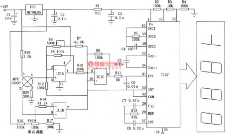
Digital Electronic Scale Composed of A/D Converter 7107
Published:2011/8/14 6:56:00 Author:Sue | Keyword: Digital, Electronic Scale, Converter
View full Circuit Diagram | Comments | Reading(4289)
Frequency Shift Modulator Composed of CA3020,MC723
Published:2011/8/18 7:58:00 Author: | Keyword: Frequency Shift, Modulator

The circuit's main component uses digital integrated circuit which can be used in frequency range of 1-10kHz. Its identification precision is high so that it can detect small frequency shift as small as 1%. The picture shows the frequency shift modulator circuit. IC1 is wide frequency amplifier CA3020. It constitutes the circuit's input terminal whose differential output are put on IC2(JK trigger MC723)'s J,K input terminals. GATE circuit IC3 constitutes monostable multivibrator, and its timing cycle is equal to half period of central frequency. Its input signal will gate the trigger after it is time delayed by the monostable multivibrator. (View)
View full Circuit Diagram | Comments | Reading(647)
| Pages:540/2234 At 20521522523524525526527528529530531532533534535536537538539540Under 20 |
Circuit Categories
power supply circuit
Amplifier Circuit
Basic Circuit
LED and Light Circuit
Sensor Circuit
Signal Processing
Electrical Equipment Circuit
Control Circuit
Remote Control Circuit
A/D-D/A Converter Circuit
Audio Circuit
Measuring and Test Circuit
Communication Circuit
Computer-Related Circuit
555 Circuit
Automotive Circuit
Repairing Circuit