
Circuit Diagram
Index 525
A newly linear matrix CCD circuit based on the single chip machine
Published:2011/8/23 22:39:00 Author:qqtang | Keyword: linear matrix, single chip machine

System formation This system is used to test the polarizing angle of the oars while the propeller is rotating. As the propeller has its rigidity, so it is not only swinging while rotating, but also shaking. To test its polarizing angle, the transient position of the propeller is be got, by using the imaging feature of CCD, the position information of the propeller is pictured by CCD, the light signal is switched into the electric signal, after passing the signal processing circuit, the signal is turned into digital signal which is conveyed to the CPU.
(View)
View full Circuit Diagram | Comments | Reading(1110)
Additional simple TV remote control circuit (LM555, CD4017)
Published:2011/8/26 1:45:00 Author:TaoXi | Keyword: Additional, simple, TV, remote control
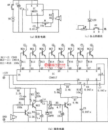
The additional simple TV remote control circuit is as shown in the figure. This circuit is composed of the launch circuit and the receiving circuit. The core of the launch circuit is the astable multivibrator which is composed of the time-base circuit 555 and the R2, W, C2, the oscillation frequency is decided by the R2, W, C2. The receiving circuit is composed of the amplification, rectification, counter circuit. The IC(CD4017) is the decimal counter/pulse distributor. The pin-9 outputs the Q8 and adds it to the pin-15 of the reset port. The CD4017 will output the Q0~Q7 which have the high level.
(View)
View full Circuit Diagram | Comments | Reading(3298)
TV power saving remote control shutdown circuit (CIC2851)
Published:2011/8/26 1:52:00 Author:TaoXi | Keyword: TV, power saving, remote control, shutdown circuit
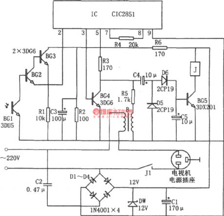
The TV power saving remote control shutdown circuit is as shown in the figure. This circuit is composed of the power supply circuit, the infrared receiver circuit, the music integrated circuit and the IC(CIC2851). When the handheld remote controller sends the signal to the TV, the phototransistor BG1 receives this signal. This signal is the pulse modulated signal, the average power is small. This signal is amplified by the BG2 to trigger the IC and makes the IC sends out the audio signal, this audio signal is rectified by D5 and D6 to produce the bias current, the bias current makes the BG5 conduct, and the relay J will close to connect the power supply of the TV.
(View)
View full Circuit Diagram | Comments | Reading(1585)
Water tower water level wired telemetry remote control device
Published:2011/8/26 2:01:00 Author:TaoXi | Keyword: Water tower, water level, wired, telemetry, remote control

The water tower water level wired telemetry remote control device is as shown in the figure. This wired telemetry remote control device has two monitor duty parts. This circuit can monitor the water level of the tower, and it can control the water level to ensure the normal water supply and water saving , so it has the certain using value.
(View)
View full Circuit Diagram | Comments | Reading(2200)
Electromagnetic valve driving circuit composed of the optical coupler
Published:2011/8/26 0:43:00 Author:TaoXi | Keyword: Electromagnetic valve, driving circuit, optical coupler

The electromagnetic valve driving circuit composed of the optical coupler is as shown in the figure. In this circuit, the TLP521-1 optical coupler isolates the input circuit and output circuit, the input circuit is the TTL level circuit, the output is the AC 220V electromagnetic valve, also the output can use the relay to control.
(View)
View full Circuit Diagram | Comments | Reading(1583)
The 300MSPS high-speed 10-bit D/A converter AD9751
Published:2011/8/23 22:39:00 Author:qqtang | Keyword: 300MSPS, D/A converter


AD9751 is produced with advanced low-cost 0.35mm CMOS skill. It can work under the voltage of 2.7V~3.6V and its power consumption is lower than 300mW. The features of AD9751 are as follows:It is one of high-speed TxDAC+s, and it is compatible with pins of other chips, it can provide with resolution ratios of 10, 12 and 14-bit.It has an ultra-high-speed converter ratio of 300MSPS.It has a dual 10-bit lock storage and multi-line multiplex input terminal.It contains the clock multipler, which can be input with differentiation and single terminal clock.
(View)
View full Circuit Diagram | Comments | Reading(636)
The ladder wave generator circuit composed of the SN74163
Published:2011/8/26 2:14:00 Author:TaoXi | Keyword: ladder wave, generator
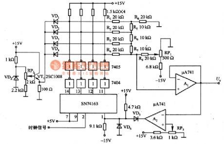
The ladder wave generator circuit composed of the SN74163 is as shown in the figure. In this circuit, the SN74163 is the synchronous counter which is the same as the clock, it can choose the frequency dividing ratio, so this device is very convenient. The VDZ and VT1 are the reference power supply that can supply the reference voltage to the D/A converter. The R1~R9 are the ladder-shaped D/A converter, it changes the input digital quantity into the analog voltage. The 7404 and 7405 are the buffer; A2 is the comparator; A1 is the outputbuffer, it outputs the step-wave voltage. RP1 is the step 1 regulation voltage; RP2 can be used to adjust the maximum voltage of the step; RP3 can be used to adjust the number of the step.
(View)
View full Circuit Diagram | Comments | Reading(1225)
Pulse generator circuit composed of 74121
Published:2011/8/26 2:27:00 Author:TaoXi | Keyword: Pulse, generator
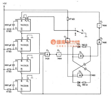
The pulse generator circuit composed of 74121 is as shown in the figure. In this circuit, the 74121(1)~74121(4) are the monostable multivibrator, the σ of the 74121(1) adds to the B port of the 74121(2), similarly, the σ of the 74121(2) adds to the B port of the 74121(3). The σ of the 74121(4) gets through the G6 and G7 gate circuits to go back to the input B of the 74121(1). When the power is connected or there is the external noise, the 74121(1)~74121(4) will produce the oscillation, the σ is in the high level stable state, and the G3 gate circuit detects the σ output of the monostable multivibrators. The G3 output signal is inversed by G4 to control the G1 and G2 to form the oscillation of the unsteady many harmonic oscillator.
(View)
View full Circuit Diagram | Comments | Reading(2310)
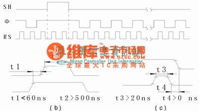
Remote control robot circuit
Published:2011/8/26 2:50:00 Author:TaoXi | Keyword: Remote control, robot
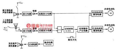
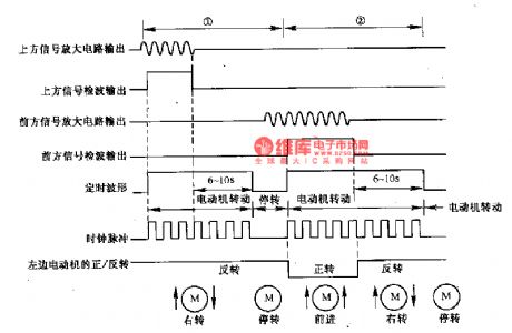
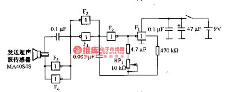

The remote control robot circuit is as shown in the figure. The figure 2-36(a) is the circuit diagram, the figure 2-36(b) is the operating timing diagram. The rotation process of the rebot is: in the circuit, the ultrasonic launching circuit is composed of the 40kHz oscillating circuit and driving circuit. The two sensors receive the ultrasonic wave: one receiving sensor is installed in the upper part of the robot; another receiving sensor is installed in front of the rebot.
In region 1, the ultrasonic sensor receives the ultrasonic wave signal and the signal is amplified by the amplifier circuit, then it is detected by the diode, at last it changes into the logic level to drive the timing circuit.
(View)
View full Circuit Diagram | Comments | Reading(2497)
Long cycle sawtooth wave generator circuit composed of the CD4020A
Published:2011/8/26 3:13:00 Author:TaoXi | Keyword: Long cycle, sawtooth wave, generator
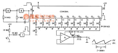
The long cycle sawtooth wave generator circuit composed of the CD4020A is as shown in the figure. The CD4O2OA is designed as the 14-level binary counter, the output port of it is connected with the R-2R trapezoidal network, it can output the analog voltage according to the clock pulse in the D/A conversion, at this time, it changes into the D/A converter. The R-2R trapezoidal network has the small resistance value, and the error is large, so we use the 200kΩ resistor. This circuit uses the 11-bit of the Q1~Q14 of CD4020A, the minimum resolution is 5/2048(V), the Q1~Q3 can be used as the frequency divider only. The oscillation period of this circuit is set to 1h, you can change the oscillation period by setting the oscillation frequency.
(View)
View full Circuit Diagram | Comments | Reading(1748)
sixteen pulses generator circuit composed of the SN74123
Published:2011/8/28 20:18:00 Author:TaoXi | Keyword: sixteen pulse, generator
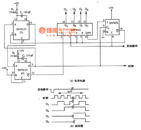
The sixteen pulses generator circuit which is composed of the SN74123 is as shown in the figure. When you input the negative pulse starting signal, it will produce the 1.2μS sixteen pulses, and the negative edge of the pulse controls the end of the counting, so we get the output of the counter. If you decode the output of the counter and use the pulse as the timing, so you can control the order of synchronous circuit.
The figure 6-40(a) shows the practical circuit, it is composed of the multivibrator which is composed of the SN74123 and SN7476, the counter which is composed of the SN74161, the start/stop control part of the counter.
(View)
View full Circuit Diagram | Comments | Reading(2615)
PLL pulse generator circuit composed of the TC5082
Published:2011/8/28 20:32:00 Author:TaoXi | Keyword: PLL, pulse, generator circuit
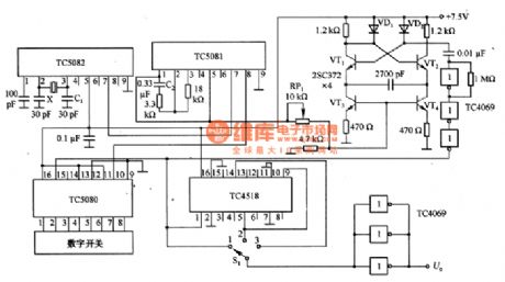
The PLL pulse generator circuit which is composed of the TC5082 is as shown in the figure. In this circuit, the x is the l0.24MHZ crystal oscillator, you can get the 10kHz reference frequency through the TC5082, and you can use the C1 to adjust the reference frequency. VT1~VT4 are the voltage-controlled oscillator, it is designed as the emitter coupling multivibrator, you can change the value of RP1 to make it oscillate in the range of 100~990kHZ. The output of the voltage-controlled oscillator is amplified by the TC4069, the amplified signal adds to the clock input port of the TC5080 (pin-15). The frequency divider circuit uses the TC4518, the output port has the buffer which is composed of the three inverter of the TC4069, the purpose of the parallel connection is to improve the driving capability.
(View)
View full Circuit Diagram | Comments | Reading(2604)
Motorcycle color changing flashing taillight
Published:2011/8/26 3:27:00 Author:TaoXi | Keyword: Motorcycle, color changing, flashing taillight

The Motorcycle color changing flashing taillight is as shown in the figure. The flashing taillight is composed of the red and green lights. In the normal driving, the red and green lights will turn on one by one. When the motorcycle is braking, all the green lights will turn off, all the red lights will trun on.
(View)
View full Circuit Diagram | Comments | Reading(667)
Brake light monitoring circuit
Published:2011/8/26 3:30:00 Author:TaoXi | Keyword: Brake light, monitoring circuit

View full Circuit Diagram | Comments | Reading(702)
Sawtooth wave generator circuit composed of the NE555
Published:2011/8/28 20:49:00 Author:TaoXi | Keyword: Sawtooth wave, generator circuit
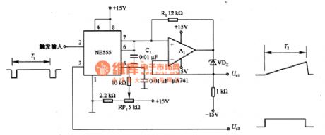
The sawtooth wave generator circuit which is composed of the NE555 is as shown in the figure. It uses the NE555 to charge the timing capacitance to produce the sawtooth wave. In the figure 6-38(a), the follower which is composed of A1 uses the bootstrap mode, the charging current of C1 is decided by the voltage-regulator diode VDZ and the resistor R1. Because the bootstrap mode is different with the mueller integral circuit, the power supply which supplies the power to the C1 is in the floating State, so it will not influences by the changing of the power supply voltage.
You can change the value of R1 or C1 by changing the cycle of the sawtooth wave, also you can use the voltage-regulator diodes with different values to change the cycle of the sawtooth wave.
(View)
View full Circuit Diagram | Comments | Reading(2339)
Function generator circuit composed of the AD7520
Published:2011/8/28 22:40:00 Author:TaoXi | Keyword: Function generator
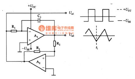
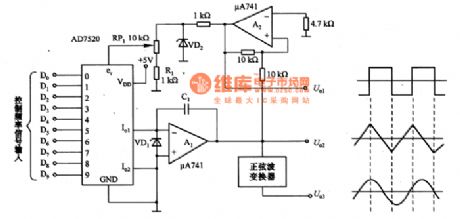
The function generator circuit which is composed of the AD7520 is as shown in the figure. The function generator basic circuit which is as shown in figure 6-37(a) is composed of the integrator A1 and the comparator A2. In the moment of T1, if the output of A2 reaches the negative saturation voltage-Uss, the output of A1 will be U. When 1+U2=0, the output of A2 will reverse, the -Uss will change into the +Ucc, the output of A1 will decrease to U. When 1+U2=0, it will reverse again. The circuit will produce the oscillation, the time constant is decided by the T=R1C1. So we can control the frequency oscillation by changing the value of R1.
(View)
View full Circuit Diagram | Comments | Reading(2383)
Sawtooth wave generating circuit composed of the μA741
Published:2011/8/28 22:51:00 Author:TaoXi | Keyword: Sawtooth wave, generating circuit
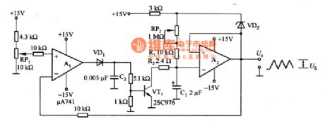
The sawtooth wave generating circuit which is composed of the μA741 is as shown in the figure. It is composed of the bootstrap circuit and the comparator. If Us is 10V, the C1 will not be charged. The output of A1 will be clamped to negative value, the VT1 cuts off. Because the output of A2 is zero, so the stable voltage power supply Uz of VD2 will add to RP2 and R1, there is the constant current. The constant current charges C1, because the A2 is the voltage follower, the output voltage of A2 is the same as the voltage of C1. The voltage of RP2 and R1 is decided by the VDZ, so the constant current continues to charge the C1. The output voltage of A2 increases linearly with the time.
(View)
View full Circuit Diagram | Comments | Reading(803)
Sawtooth wave generating circuit composed of the LM301
Published:2011/8/28 23:03:00 Author:TaoXi | Keyword: Sawtooth wave, generating circuit
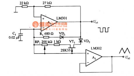
The sawtooth wave generating circuit which is composed of the LM301 is as shown in the figure. The timing resistor of the multivibrator is devided by VD1 and VD2, and it uses the charging and discharging voltage of C1 to produce the sawtooth wave. A1 is the level comparator, when the output of it is positive, the VD1 cuts off, the VD2 conducts, the current which is added to C1 is produced by the constant current source which is composed of VT1, so the voltage straights up. When the output of A1 is negative, the VD2 cuts off, the VD1 conducts, the timing resistor changes into R1, the fall time is less than the rise time. The voltage of C1 is the sawtooth wave voltage, it is output by the buffer amplifier A2.
(View)
View full Circuit Diagram | Comments | Reading(1838)
Broadband function generator circuit
Published:2011/8/29 1:25:00 Author:TaoXi | Keyword: Broadband, function, generator
The broadband function generator circuit is as shown in the figure, the frequency range is 1HZ~1MHZ. In the circuit, the A2 is operating in the voltage follower state and it has the buffer function. A3 is the high-speed comparator that can be used to detect the positive and negative amplitude of the triangle wave output waveform, it switches the control voltage which is added on the constant current source. A1 is the program-controlled constant current source, the output DC adds to the RC network, and this output DC is integrated to be the triangle waveform.
The C1~C3 can be used to adjust the output waveform of the triangle wave, you can get the triangle waveform with good linearity by adjusting the three capacitors in the range of 5OOkHZ~1MHz.
(View)
View full Circuit Diagram | Comments | Reading(2169)
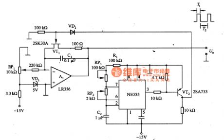
Triangular wave generation circuit with the adjustable amplitude
Published:2011/8/29 2:09:00 Author:TaoXi | Keyword: Triangular wave, generation circuit, adjustable amplitude
The triangular wave generation circuit with the amplitude that can be adjusted accurately is as shown in the figure, the accuracy of the amplitude is +/-0.01V, if you add the +UREF and -UREF DC voltage, the amplitude of the triangular wave can be the positive and negative peak values.
The circuit is composed of the integrator which is composed of A1, the positive and negative peak values judgment comparators A2 and A3. The U1 outputs the triangular wave, the U2 outputs the square wave. You can change the frequency of the output signal by changing the value of R1. The symmetrical characteristic of the waveform can be adjusted. At this time, you can connect the potentiometer RP1 with the positive and negative power supplies (figure 6-29(b)).
(View)
View full Circuit Diagram | Comments | Reading(873)
| Pages:525/2234 At 20521522523524525526527528529530531532533534535536537538539540Under 20 |
Circuit Categories
power supply circuit
Amplifier Circuit
Basic Circuit
LED and Light Circuit
Sensor Circuit
Signal Processing
Electrical Equipment Circuit
Control Circuit
Remote Control Circuit
A/D-D/A Converter Circuit
Audio Circuit
Measuring and Test Circuit
Communication Circuit
Computer-Related Circuit
555 Circuit
Automotive Circuit
Repairing Circuit