
Circuit Diagram
Index 539
PT-8820 "idiot" type record-replay audio integrated circuit
Published:2011/7/23 2:56:00 Author:chopper | Keyword: "idiot" type, record-replay, audio, integrated circuit

PT-8820 is the audio product of PT series.The product uses an advanced level to directly simulate the flash memory technology, and it can provide nonvolatile sound or data storage without A/D, D/A converter, which can provide high-quality audio playback, and can catch up with digital recording effect. PT-8820 does not need back-up battery, and the recording information will not lost when the power is off. As a result ofthe unique bi-directional analog I/O speech switching technology, PT-8820 can use the speaker as a microphone for recording,which is easy to form the simplest sound recording circuit. (View)
View full Circuit Diagram | Comments | Reading(1553)
HT8656 record and playback integrated circuit
Published:2011/7/23 3:03:00 Author:chopper | Keyword: record, playback, integrated circuit

In the HT8656 record and play back voice IC there is a sound auto-detection circuit.When the circuit is in a wait state, the microphone receives a sound signal,and the circuit will automatically enter the recording state;when the sound stops (or be silent) about 1s, the circuit will automatically turn the recording state into playback state, and it will automatically return to the wait state after the end of the playback.It is used for voice-operated words learning toys, arts and crafts. Typical application circuit is shown as picture. (View)
View full Circuit Diagram | Comments | Reading(1713)
AN7025K/7025S AM/FM stereo radio circuit
Published:2011/7/23 2:39:00 Author:chopper | Keyword: AM/FM, stereo, radio circuit

View full Circuit Diagram | Comments | Reading(4060)
TA7641BP low-consumption AM radio circuit
Published:2011/7/23 2:35:00 Author:chopper | Keyword: low-consumption, AM, radio circuit

View full Circuit Diagram | Comments | Reading(2356)
Transistor Arithmetic Product Wave Detector Circuit
Published:2011/8/23 23:41:00 Author:Robert | Keyword: Transistor, Arithmetic, Product, Wave, Detector
The picture shows the arithmetic product wave detector circuit composed of dual-electrode transistor. The action of the circuit likes a amplifier. But the base electrode of the transistor is controlled by the local oscillator. The SSB signal would input from the T1's low-impedance secondary coil and then it should be normally amplified by Q1. But the local oscillator inhibiting action stop this process. The local oscillator controls the transistor connected or disconnected. It produces the nonlinear feature needed by demodulation.
The picture shows the transistor arithmetic product wave detector circuit. (View)
View full Circuit Diagram | Comments | Reading(919)
CD4520 digital coded lock circuit
Published:2011/7/25 2:49:00 Author:chopper | Keyword: digital, coded lock

Figure shows the general-purpose digital coded lock circuit formed by the CMOS digital integrated circuit, which is characterized by a wide supply voltage range, low power consumption, anti-jamming performance, fewer external components.There are 256 password combinations, and it is of pseudo-code switch, and has a good security feature, the circuit is shown as figure.The coded lock circuit consists of a dual-binary synchronous add counter CD4520,and there are two binary counters of same structure in the circuit.
(View)
View full Circuit Diagram | Comments | Reading(1813)
Dual JFET Arithmetic Product Wave Detector Circuit
Published:2011/8/23 23:41:00 Author:Robert | Keyword: Dual, JFET, Arithmetic, Product, Wave, Detector
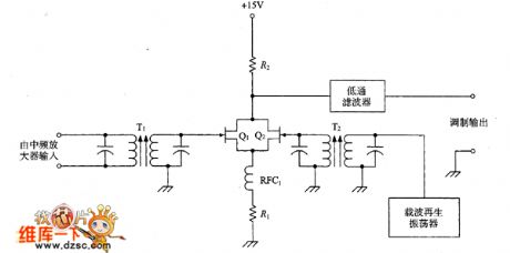
In the picture, it uses a couple of differencial signal junction type FET (JFET) to generate the arithmetic product wave detection. The SSB signal is added to the Q1's grid electrode. The local oscillator is used to interrupt the circuit in the Q2 side. It should note that the local oscillator's signal amplitude is much stronger than the SSB signal. The two tubes' common drain electrode circuit is connected to a low-pass filter and then it connects the output port. The filter is adjusted to the spectra which is needed to be overlayed (usually it is the audio frequency).
The picture shows the dual JFET arithmetic product wave detector circuit. (View)
View full Circuit Diagram | Comments | Reading(1337)
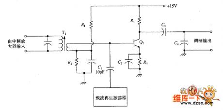
MOSFET Arithmetic Product Wave Detector Circuit
Published:2011/8/23 23:41:00 Author:Robert | Keyword: MOSFET, Arithmetic, Product, Wave, Detector
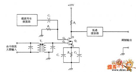
The circuit shown in the picture a MOSFET with dual grid electrodes: the G1's normal signal input is used to receive the SSB signal from the IF amplifier; the G2's local oscillator signal would control the MOSFET's switch. The audio low-pass filter is also in the output (drain electrode) circuit to limit the redundant IF signal from the demodulator output.The picture shows the MOSFET arithmetic product wave detector circuit.Notes: in this circuit the MOSFET's source circuit has two capacitance (C1 and C2). Typically one is RF capacitance and the other is AF capacitance. Although using the modern capacitors, this distinction is not very necessary. (View)
View full Circuit Diagram | Comments | Reading(950)
MC-1496 Arithmetic Product Wave Detector Circuit
Published:2011/8/23 23:41:00 Author:Robert | Keyword: Arithmetic, Product, Wave, Detector
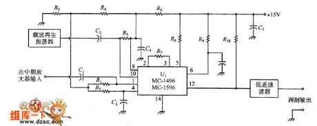
The picture shows a integrated SSB arithmetic product wave detector circuit. The circuit is based on the MC-1496 analog multiplier chip. It contains a transconductance unit demodulator whose switch is controlled by a local oscillator. The SSB mid-frequency signal would input to the pin 1 and the local oscillator would input to the pin 10. Other pins would be added the corresponding bias voltage according to different working conditions or not used.
The picture shows the MC-1496 arithmetic product wave detector circuit. (View)
View full Circuit Diagram | Comments | Reading(2369)
Dual Tuning Frequency Detector Circuit
Published:2011/8/23 23:41:00 Author:Robert | Keyword: Dual, Tuning, Frequency, Detector
A classic FM frequency detector circuit is shown in the picture. The circuit uses a special transformer which has two secondary windings. The two secondary windings are separately connected to the two sides of the IF frequency which have the same distance to IF frequency and are not fay from the IF frequency. The two frequency's distance should be a little bigger than the transmitter's amplitude. The output would combine through a couple differencial signal diodes (D1 and D2). The diodes' output ports are connected to the load resistor R1 and R2. Generally, when the signal has not been modulated, the algebraic sum of the two diodes' output is zero. That would make the output be zero. (View)
View full Circuit Diagram | Comments | Reading(928)
Single-Phase Half-Wave Rectifier Circuit
Published:2011/8/23 23:41:00 Author:Robert | Keyword: Single, Phase, Half, Wave, Rectifier

Common used low-power rectifier circuits has single-phase half-wave rectifier circuit, single-phase full-wave rectifier circuit and single-phase bridge rectifier circuit. Because the single-phase bridge rectifier circuit has good performance, it is one of the most common used rectifier circuits.The picture shows the single-phase half-wave rectifier circuit and working waveform. In the circuit shown in the picture, the transformer T1 would be convert the commercial electricity AC 220V U1 to the needed AC voltage U2. The rectifier diode VD would convert the transformer secondary voltage U2 to single-direction conducted DC voltage. (View)
View full Circuit Diagram | Comments | Reading(1263)
Single-Phase Full-Wave Rectifier Circuit
Published:2011/8/23 23:41:00 Author:Robert | Keyword: Single, Phase, Full, Wave, Rectifier

The picture shows the full-wave rectifier circuit and working waveform. From the circuit shown in the picture, we know that this circuit connects two rectifier diode to the transformer T1's secondary winding middle tap to make them work alternately. The * signal means the transformer's corresponding terminals. The transformer's two secondary voltage has the equal value. (View)
View full Circuit Diagram | Comments | Reading(1426)
Capacitance Filter Circuit
Published:2011/8/23 23:41:00 Author:Robert | Keyword: Capacitance, Filter

After the rectifier the output voltage would change to be DC voltage, but the voltage waveform fluctuate largely. In order to get the smoothing DC voltage waveform, it needs to use the filter method. The filter method is always using the performance of the reactance feature from the reactance components to the AC signals. And it would connect the capacitance or inductance to the load resistance to make up the filter circuit.The picture shows the single-phase half-wave rectifier capacitance filter circuit and working waveform. From the picture (a), when the circuit is not connectted to the capacitance C, the output voltage would be shown in dotted line of picture (b). (View)
View full Circuit Diagram | Comments | Reading(667)
Inductance Filter Circuit
Published:2011/8/23 23:41:00 Author:Robert | Keyword: Inductance, Filter

The capacitance filter circuit's output internal resistance is very big. When the RL changing, the port voltage would also change. Also, the when current-limiting diode is conducted, the impact current is very large which would effect its life. The resistance is small but its AC impedance is very large, that is the inductance filter circuit. So it could use the inductance coil for DC voltage, which is the inductance filter. The picture shows some inductance filter circuit.
The picture shows the inductance filter circuit.
The picture (a) shows the single inductance filter circuit. Its weakness is: generally its filter coefficient (the filter coefficient is the first harmonic voltage amplitude ratio between the filter circuit input port and output port) could only be made under several dozens. (View)
View full Circuit Diagram | Comments | Reading(751)
Voltage Regulator Circuit Composed Of Zener Diodes
Published:2011/8/23 23:40:00 Author:Robert | Keyword: Voltage, Regulator, Zener, Diode

The picture shows the voltage regulator circuit composed of zener diodes. And, the picture (a) shows the circuit with output of 6V/50mA. Now it introduces the determining method of the each components in the circuit. The input voltage U is 10V~16V, and at this time the output voltage Uo=Uz-UBE. The transistor VT1's UBE is fixed which is about 0.65V. So the VS's stable voltage is Uz=6V+0.65V=6.65V. It could use the RD6.8EB1 zener diode.The picture shows the voltage regulator circuit composed of zener diodes.(a)The circuit with output of 6V/50mA. (b)The circuit which using LEDs to replace the zener diodes. (c)The circuit which using the resistance for voltage dividing. (d) The voltage regulator circuit which has the best performance. (View)
View full Circuit Diagram | Comments | Reading(2362)
Transistor Basic Voltage Regulator Circuit
Published:2011/8/23 23:40:00 Author:Robert | Keyword: Transistor, Basic, Voltage, Regulator

The transistors series voltage regulator circuit is shown in the picture. And, the picture (a) is equivalent circuit. The VT1 is adjustment transistor which is used to adjust the output voltage. The VT1 and load RL are in series. So this circuit is called the series voltage regulator circuit. Because the adjustment tube is using the transistors, the transistor series voltage regulator circuit could work under a big working current which could overcome the weakness that the zener diode regulator circuit's output current is limited by the zener diode limiting current. The picture (b) is the practical series voltage regulator circuit. The picture (c) is its diagram circuit. (View)
View full Circuit Diagram | Comments | Reading(983)
Voltage Regulator Circuit With Auxiliary Power
Published:2011/8/23 23:40:00 Author:Robert | Keyword: Voltage, Regulator, Auxiliary, Power

The circuit shown in picture (b) can not stabilize well for the transient voltage. Because this transient voltage could be through the resistance R4 and add to the output port through the amplification of the adjustment tube. Also in the circuit shown in picture (b), the amplifier's power, which is the input voltage U1, is also not stabilized. So it could add the R4 directly to the power input port and make the amplifier's power stable, which is shown in picture (a). But in order to make the zener diode VS2 work normally in the circuit, it must make the adjustment tube VT1's tube voltage drop UCE larger than the VS2's working voltage. This would increase the VT1's power consumption. (View)
View full Circuit Diagram | Comments | Reading(723)
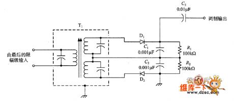
Sixteen sound phonation circuit with CD4011,CD4066
Published:2011/7/22 2:55:00 Author:chopper | Keyword: Sixteen sound, phonation circuit

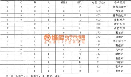
Sixteen sound phonation circuit adopts another analog phonation circuit KD9561.In accordance with internal fixed process of the circuit, there are 4 analog sound in the KD9561,such as machine gun sound, siren, ambulance soundand fire engine sound.It has two sound trigger ends SEL1 and SEL2, andthey can be triggered by high, low level or floatingthey respectively.
(View)
View full Circuit Diagram | Comments | Reading(4484)
digital coded lock circuit with CD4520
Published:2011/7/22 3:29:00 Author:chopper | Keyword: digital, coded lock

Figure shows the general-purpose digital coded lock circuit formed by the CMOS digital integrated circuit, which is characterized by a wide supply voltage range, low power consumption, anti-jamming performance, fewer external components.There are 256 password combinations, and it is of pseudo-code switch, and has a good security feature, the circuit is shown as figure.The coded lock circuit consists of a dual-binary synchronous add counter CD4520,and there are twobinary counters of same structure in the circuit.
(View)
View full Circuit Diagram | Comments | Reading(2952)
Voltage Adjustable Circuit
Published:2011/8/23 23:41:00 Author:Robert | Keyword: Voltage, Adjustable

The modern mobile electronic devices is more easier to have this problem than the inchoate devices. In the communication devices and the FM radio, the oscillator voltage is controlled specially. The picture (a) shows the zener diode controller which is used in many car radio circuits. The picture (b) shows a three-segment voltage controller. It could control the mobile transmitter oscillator voltage in 10V. If these controlling components have errors, the circuit would have the frequency drifting. So that the nominal 12V car power is practically unstable. (View)
View full Circuit Diagram | Comments | Reading(612)
| Pages:539/2234 At 20521522523524525526527528529530531532533534535536537538539540Under 20 |
Circuit Categories
power supply circuit
Amplifier Circuit
Basic Circuit
LED and Light Circuit
Sensor Circuit
Signal Processing
Electrical Equipment Circuit
Control Circuit
Remote Control Circuit
A/D-D/A Converter Circuit
Audio Circuit
Measuring and Test Circuit
Communication Circuit
Computer-Related Circuit
555 Circuit
Automotive Circuit
Repairing Circuit