Circuit Diagram
Index 526
Ladder wave generation circuit composed of the LM3900
Published:2011/8/28 19:51:00 Author:TaoXi | Keyword: Ladder wave, generation circuit

The ladder wave generation circuit composed of the LM3900 is as shown in the figure. The A1 forms the oscillation part of the ladder wave input pulse through the resistor R1. A2 has the integral and holding functions and it can get the ladder wave from the output. A3 and A4 have the functions of the comparator circuit and the monostable multivibrator.
R2 can be used in the sampling of the ladder wave's output, it compares with the power supply voltage +Ucc through the resistor R3. When the output voltage of A2 is more than 80% of +Ucc, the A3 and A4 produce the 100μs reset pulse, and it makes the output of the integrator A2 to 0V.
(View)
View full Circuit Diagram | Comments | Reading(1542)
Ladder wave generation circuit
Published:2011/8/29 1:37:00 Author:TaoXi | Keyword: Ladder wave, generation circuit

The ladder wave generation circuit is as shown in the figure. In this circuit, the A1 is the multivibrator which produces the square wave, and it is controlled by the 8-pin of the selective passing port. A2 is the integrator, the output of it is the ladder wave, the operating state of it is controlled by the delay switch. A3 is the delay amplifier, it makes the output of selective passing port's 8-pin divide by R1 and R2, and it adds the positive feedback to pin-2 to make it have the delay characteristic. The C1 can be used to adjust the frequency of the multivibrator, the C2 can be used to adjust the stepping height, the VD1 can be used to prevent the reversal of the multivibrator, VD2 and VD3 are the charging commutation circuit.
(View)
View full Circuit Diagram | Comments | Reading(824)
Triangle wave generator uses the luminous flux to change the frequency
Published:2011/8/28 20:03:00 Author:TaoXi | Keyword: Triangle wave, generator, luminous flux, frequency

Triangle wave generator which uses the luminous flux to change the frequency is as shown in the figure. A part of the timing resistor of the function generator uses the photoconductive resistance RG to change the frequency through the luminous flux. The complementary re-flip flop which is composed of VT1 and VT2 inspires the RG. The resistance attenuator is composed of the R1, R2 and R3 that can be used to improve the input impedance of μPC55A, and it makes the frequency extend upward. The RP2 can be used to adjust the symmetrical characteristic of the output amplitude.
(View)
View full Circuit Diagram | Comments | Reading(882)
Voltage-controlled oscillator circuit
Published:2011/8/29 1:52:00 Author:TaoXi | Keyword: Voltage-controlled, oscillator circuit

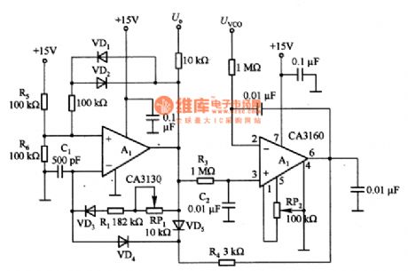
The voltage-controlled oscillator circuit is as shown in the figure. The input voltage range of the oscillator is 0-10V, the change sensitivity is 1kHz/V, the tracking error is 0.02%, the temperature coefficient is 0.01%. The multivibrator is composed of A1 that can produce the constant amplitude and constant pulse width rectangular wave, the output amplitude is the positive and negative power supply voltage. The rectangular wave which is output by A1 is processed by the integration circuits R3 and C2 to be the average voltage, this average voltage adds to the in-phase inout port of the comparator A2. The A2 is in the state of the input voltage is the same as the rectangular wave average voltage, and it adds the output to the reverse-phase input port of A1 through the R4 and VD4 to change the deadline of the multivibrator.
(View)
View full Circuit Diagram | Comments | Reading(1093)
C6458 power supply circuit
Published:2011/8/26 3:32:00 Author:TaoXi | Keyword: power supply
View full Circuit Diagram | Comments | Reading(910)
Hitachi A1PM8C power supply circuit
Published:2011/8/29 2:42:00 Author:TaoXi | Keyword: Hitachi, power supply

The oscillation process
The 220V AC voltage is fully rectified by the circuit to produce the 300V DC voltage on C906, and this DC voltage adds to the pin-3 of the IC901 through the L1 winding resistor of T901, at the same time the 220V voltage is half-wave rectified by the circuit and the voltage adds to pin-2 of IC901 through the R942, R903, R904, the internal switching tube of IC901 conducts, the current of L1 of the T901 increases, the winding resistor L2 produces the positive feedback voltage, this voltage adds to the pin-2 of the IC901 through the Q901, D905, L907, so the internal switch tube of IC901 saturates quickly.
During the switch turn-on period, the winding resistor L2 charges the C905 through the R906 and R907, and it charges the C909 through the R909, the charging result of the C909 is the electric potential decreasing of the pin-1 of IC901.
(View)
View full Circuit Diagram | Comments | Reading(1681)
Hitachi A3P-B2 power supply circuit
Published:2011/8/29 3:29:00 Author:TaoXi | Keyword: Hitachi, power supply

Oscillation process
If you add the voltage which is more than 6V to the pin-9 of STR6709, the switch power supply will start oscillating.
The voltage of C907 is about 300V, it adds to the C electrode of the IC901's pin-1 internal switch tube through the P1 and P2 winding resistors, and the 220V AC is rectified by D908, then it is limited by R903 and R917 and filted by C909 to be the unstable DC voltage, this DC voltage adds to the pin-9 of IC901, the switch power supply starts oscillating. After the power supply is started, the induced voltage of V1 and V2 are rectified by D903 to be the 9.5V voltage, and it supplies the power to pin-9 of IC901. Q901 is intended for the power supply of IC901's pin-9 in the standby state.
(View)
View full Circuit Diagram | Comments | Reading(2340)
+5V input +30V output boost circuit
Published:2011/8/29 3:48:00 Author:TaoXi | Keyword: +5V, input, +30V, output, boost circuit

The +5V input +30V output boost circuit
(View)
View full Circuit Diagram | Comments | Reading(1064)
LM317 integrated voltage regulator circuit
Published:2011/8/29 3:36:00 Author:TaoXi | Keyword: integrated voltage, regulator circuit

The LM317 is designed as the common adjustable integrated voltage regulator with the maximum output current of 2.2A, the output voltage range is 1.25-37V. The connection method is:
The reference voltage between pin-1 and pin-2 is 1.25V. In order to ensure the output voltage stabilizer performance, R1 is smaller than 240ohms. You can adjust the voltage regulator value by adjusting the value of R2. The D1 and D2 can be used to protect the LM317.
Uo=(1+R2/R1)*1.25
The LM317 integrated voltage regulator circuit (View)
View full Circuit Diagram | Comments | Reading(1302)
300VA UPS computer power supply circuit
Published:2011/8/29 3:46:00 Author:TaoXi | Keyword: 300VA, UPS, computer, power supply
View full Circuit Diagram | Comments | Reading(3608)
A3 power supply circuit
Published:2011/8/29 3:43:00 Author:TaoXi | Keyword: power supply
View full Circuit Diagram | Comments | Reading(934)
IX0689 power supply circuit
Published:2011/8/29 3:43:00 Author:TaoXi | Keyword: power supply
View full Circuit Diagram | Comments | Reading(997)
The clock synthesizer circuit composed of the MC74HC4046
Published:2011/8/29 3:41:00 Author:TaoXi | Keyword: clock synthesizer

The clock synthesizer circuit which is composed of the MC74HC4046 is as shown in the figure, it can produce the 1MHZ~2OMHZ high precision clock signal. The output A is the 1MHZ~2OMHZ signal with the resolution ratio of 100kHz, the output B and output C outputs the signal with the 1/10 frequency respectively. If the input signal Vi is the 10kHz frequency demultiplication signal of the crystal circuit, the frequency precision of this circuit is the same as the crystal oscillator.
(View)
View full Circuit Diagram | Comments | Reading(2894)
The LED flashing circuit
Published:2011/8/13 2:10:00 Author:qqtang | Keyword: LED flashing circuit
View full Circuit Diagram | Comments | Reading(1106)
The ultra-sonic liquid level indicating circuit composed of NE555
Published:2011/8/23 22:40:00 Author:qqtang | Keyword: ultra-sonic, liquid level, indicating circuit

In the figure is the ultra-sonic liquid level indicating circuit. The circuit consists of the ultra-sonic emitting circuit and receiving circuit. The ultra-sonic emitting circuit consists of the 555, R1, W1, C1 and ultra-sonic emitting head UCM40T. The ultra-sonic receiving circuit consists of the receiving head UCM40R compatible with the emitting head, cascade amplifiers BG1 and BG2 and the test circuit. When the liquid level is approaching the receiving head, the voltmeter deflection angle is rising up, and the closer the liquid level is, the bigger the deflection angle will be. (View)
View full Circuit Diagram | Comments | Reading(639)
The switch power supply:Hitachi A3P-B2 power supply
Published:2011/8/13 2:12:00 Author:qqtang | Keyword: Hitachi, switch power supply
View full Circuit Diagram | Comments | Reading(819)
The analog thermistor composed of the current outputting precise integrated temperature sensor AD590
Published:2011/8/23 22:36:00 Author:qqtang | Keyword: analog thermistor, integrated temperature sensor

The simplest temperature test circuit composed of AD590 is shown in the figure. AD590 switches the temperature under test into current, which makes the microamp meter deflect. After the meter is marked, it can be used as the analog thermometer. To avoid the disturbance from the outside, the outgoing line should be the double stranded wire(stranded wire for short), and its length could be several hundred. (View)
View full Circuit Diagram | Comments | Reading(825)
The digital thermistor composed of the current outputting precise integrated temperature sensor AD590
Published:2011/8/23 22:36:00 Author:qqtang | Keyword: digital thermistor, temperature sensor

(View)
View full Circuit Diagram | Comments | Reading(1962)
The FM-RTFQl-868/433/315 MHz FM emitter module
Published:2011/8/23 22:37:00 Author:qqtang | Keyword: emitter module


FM-RTFQl-xxx is a high-efficiency FM emitter. The types of the series are FM-RTFQl-315 MHz, FM-RTFQ1-433 MHz and FM-RTFQl-868 MHz, and its coupled receivers are FM-RRFQ1-315 MHz, FM-RRFQl-433 MHz和FM-RRFQl-868 MHz. They are fitted in the wireless secure system, car alarm and remote control/test. The features of the circuit are: the working frequency is 315/433/868 MHz; emitting distance is 250m; data transmitting speed is 9.67 Kb/s; power supply voltage is 2.1~4.0V; the maximum power supply current is 8mA, the maximum standby current is 100mA.
(View)
View full Circuit Diagram | Comments | Reading(1220)
The long-distance temperature test circuit composed of the intelligent temperature sensor TMP03
Published:2011/8/23 22:37:00 Author:qqtang | Keyword: temperature test circuit, intelligent temperature sensor

In the figure is the long-distance temperature test circuit composed of the intelligent temperature sensor TMP03. As there is a high common mode voltage on the transmission line, so the photo-coupler should be used to separate the output terminal. The circuits of the 3 photo-couplers are shown in figure (a), (b) and (c) respectively. (View)
View full Circuit Diagram | Comments | Reading(702)
| Pages:526/2234 At 20521522523524525526527528529530531532533534535536537538539540Under 20 |
Circuit Categories
power supply circuit
Amplifier Circuit
Basic Circuit
LED and Light Circuit
Sensor Circuit
Signal Processing
Electrical Equipment Circuit
Control Circuit
Remote Control Circuit
A/D-D/A Converter Circuit
Audio Circuit
Measuring and Test Circuit
Communication Circuit
Computer-Related Circuit
555 Circuit
Automotive Circuit
Repairing Circuit


