Circuit Diagram
Index 1634
555 Simple Voltage-controlled Oscillator
Published:2011/6/27 4:11:00 Author:Zoey | Keyword: 555 Simple, Voltage-controlled, Oscillator

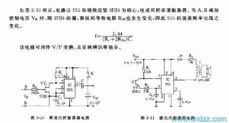
As shown in the picture 3-10, the circuit take the 555 and FET 3DJ6 as its key part to constitute a controllable multi-vibrator. As soon as terminal A and B controlled by voltage Vk, equivalent resistance between drain and source of 3DJ6 will change thereby. So, it causes the frequency change of 555.
f=1.44/(R1+2RDS)C1
This circuit can also be applied in various situations such as to transform V/F,or to identify different tones, etc. (View)
View full Circuit Diagram | Comments | Reading(1180)
Electrical blaster 1
Published:2011/6/28 2:25:00 Author:Nicole | Keyword: Electrical blaster

The electrical blaster circuit is composed of self-exciting oscillator, high voltage generation circuit, charge indication circuit and discharge circuit, it is shown in the figure 8-23.
The self-exciting oscillator circuit is made of resistors R1, R2, capacitors C1-C3, transistors V1, V2, charge switch S1, battery GB and W1, W2 windings of boost transformer T.
The high voltage generation circuit consists of W3 winding of boost transformer T, capacitors C4-C7 and rectifier diode VD1-VD4. The dual voltage rectifier circuit is made of C4, C5 and VD1-VD4.
The charge indication circuit is composed of resistors R3-R6 and neon indication light HL.
(View)
View full Circuit Diagram | Comments | Reading(811)
Loom saves electricity controller 3
Published:2011/6/29 21:41:00 Author:Nicole | Keyword: loom, saves electricity controller

The loom saves electricity controller circuit is composed of DC regulated power supply circuit, touch control circuit, automatically control circuit and master control circuit, it is shown in the figure 19.
The DC regulated power supply circuit is made of current transformer T, bridge rectifiers UR, filter capacitor C, current limiting resistor R1 and steady voltage diode VS.
The touch control circuit consists of touch electrode A, resistors R2-R4 and transistor V1.
The automatically control circuit is composed of travel switch S2, resistor R5, relay K, diode VD and transistor V2.
(View)
View full Circuit Diagram | Comments | Reading(1046)
Circuit:MP3 circuit
Published:2011/6/27 1:56:00 Author:zj | Keyword: MP3
View full Circuit Diagram | Comments | Reading(1289)
Loom saves electricity controller 2
Published:2011/6/29 21:35:00 Author:Nicole | Keyword: loom, saves electricity controller

The loom saves electricity controller circuit is composed of 12V regulated power supply circuit, current detection amplifier circuit, relay control circuit and motor control switch circuit, it is shown in the figure 8-18.
The 12V regulated power supply circuit is made of current transformer T, bridge rectifiers UR, filter capacitors C4, C5, current limiting resistor R8 and steady voltage diode VS.
The current detection amplifier circuit consists of current transformer TA, diodes VDl-VD3, capacitor C1, potentiometer RP, resistors R1-R4, transistor V1.
V1-V3's sensitivity can be changed by adjusting RP.
(View)
View full Circuit Diagram | Comments | Reading(951)
Infrared remote control heat release column circuit
Published:2011/6/27 22:19:00 Author:chopper | Keyword: Infrared, remote control, heat release, column circuit
View full Circuit Diagram | Comments | Reading(497)
TMS3450NL Digital Clock Integrated Circuit Diagram
Published:2011/7/3 1:35:00 Author:Vicky | Keyword: Digital Clock Integrated Circuit


TMS3450NLis digital clock integrated circuit produced by Toshiba Corporation. It is widely used in various kinds of digital clock and auto clock circuit.
1 internal block circuit diagram and pin funtion
Internal block circuit diagram of TMS3450NL integrated circuit and the pin function are all shown in the above picture.
Internal block circuit diagram of IC TMS345ONL
Typical applied circuit of IC TMS345ONL
(View)
View full Circuit Diagram | Comments | Reading(18656)
Circuit Diagram of Simplified Voltage Doubler Composed of Inverter
Published:2011/7/2 22:13:00 Author:Vicky | Keyword: Simplified Voltage Doubler

The above picture is a simplest voltage doubler composed of CMOS NOT-Gate CD4069. It is probably the most basic DC/DC booster circuit. 4069, R1 and C1 together constitute a multivibrator of about 100 KHz. The output of the oscillator changes form 0 to 10V. When the output is 0V, the capacitance C2 is charged to 10V via VD1; when the output of oscillator rises to +10V suddenly, because that the two ends of capacitance cannot mutate, end A of capacitance C2 correspondently rises to +20V. Under such circumstance, VDI1 is reverse biased, and the current charges the C3 via VD2, and therefore the output end’s voltage is +20V. However, because there is pressure drop in the diode , the actual output is a litter lower than +20V. (View)
View full Circuit Diagram | Comments | Reading(1647)
QM Series Gas Sensor Basic Testing Circuit
Published:2011/7/3 5:51:00 Author:Robert | Keyword: Gas, Sensor, Basic, Testing

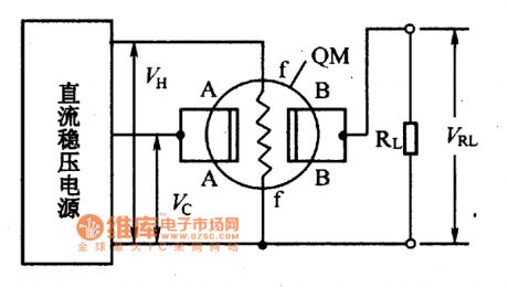
The picture shows the QM series gas sensor basic testing circuit. (View)
View full Circuit Diagram | Comments | Reading(954)
AAT3680 lithium battery linear charging integrated circuit
Published:2011/7/3 21:09:00 Author:Christina | Keyword: lithium battery, linear charging, integrated circuit


The AAT3680 is designed as one kind of lithium battery linear charging integrated circuit that can be used in cellphone, PDA, digital camera and the desktop charger.
1.Features
The charging system which is composed of the AT3680 has the function of charging voltage and charging current adjustment, also it sets the two times inrush current charging function, there is a pin to control the two times inrush current.
2.Pin functions and data
The AAT3680 has eight pins and it has three kinds of packages: MSOP、TSSOP or SOP, the pin-5 of the SOP and TSSOP has the same function and arrangement.
Table 1 The pin functions and data of the AAT3680
3.Typical application circuit
The typical application circuit of the AAT3680 is as shown in figure 1.
Table 2 The five kinds of charging state and display situations
(View)
View full Circuit Diagram | Comments | Reading(587)
2CU301 silicon photosensitive diode appearance structure and circuit
Published:2011/7/3 20:49:00 Author:Christina | Keyword: silicon, photosensitive diode, appearance structure

The 2CU301 four-quadrant silicon photosensitive diode is in the sealed metal shell package, there is the glass window on the top. The appearance structure is as shown in the figure.
Figure: 2CU301 silicon photosensitive diode appearance structure and circuit (View)
View full Circuit Diagram | Comments | Reading(570)
LA1140 IC Internal Diagram Circuit And Typical Application Circuit
Published:2011/7/3 1:09:00 Author:Robert | Keyword: IC, Internal, Diagram, Typical, Application

The LA1140 is a high-frequency middle-amplifier IC which is mainly used for radio middle-frequency signal processing in many kinds of audio equipments.
The LA1140 IC has internal middle amplifier, amplitude limiting, wave detecting, output signal voltage level indicator and other functions. Its sensitivity of amplitude limiting is high and its gain and frequency can be controlled automatically. Its automatical frequency control output can complete the noise elimination by clamping and it would vary in proportion with the size of the input signal.
The picture shows the LA1140. (View)
View full Circuit Diagram | Comments | Reading(4554)
Loom saves electricity controller 1
Published:2011/6/29 21:20:00 Author:Nicole | Keyword: loom, saves electricity controller

The loom saves electricity controller is composed of air switch QF, AC contactor KM, time relay KT, control switch S1, travel switch S2, hand brake indicator switch S3, heat relay KP and light EL, it is shown in the figure 8-17.
When the air switch QF is turned on, the loom's switch bar is pulled to start-up position, when the cam turns 5°-lO°, S2 is released, S2's normally closed contact S2-1 is turned on, time relay KT is turned on, the delay cutting normally open contact is connected, AC contactor KM pulls in, motor M starts working.
(View)
View full Circuit Diagram | Comments | Reading(990)
multipath supply output circuit
Published:2011/6/28 6:39:00 Author:chopper | Keyword: multipath supply, output circuit

The picture is a multipath supply output circuit,it will output three values of voltage like +UCC and ±UA.In the circuit,point A is the reference earthing point of positive-negative double supply;point B is the reference earthing point of positive power supply.① is the earth lead among reference potentials; ② is the reference earth lead of the regulator.
(View)
View full Circuit Diagram | Comments | Reading(531)
T5875 Ringing Integrated Circuit
Published:2011/7/3 1:18:00 Author:Robert | Keyword: Ringing, Integrated


The T5875 is a ringing IC which is widely used in the ringing circuits in many kinds of communication equipments.
1. Its pin's functions.
T5875 IC uses 8-pin dual inline package and its pin's functions is listed in table 1.
The table 1 shows the T5875 IC's pin's functions.
2.Typical application circuit.
The ringing circuit typical application circuit composed of the T5875 IC is shown in picture 1.
The picture shows the T5875 IC's typical application circuit. (View)
View full Circuit Diagram | Comments | Reading(1041)
Electric welding machine no load electricity saver 12
Published:2011/6/30 22:00:00 Author:Nicole | Keyword: electric welding machine, electricity saver

The electric welding machine no load electricity saver circuit is composed of current detection circuit, power supply circuit and switch control circuit, it is shown in the figure 8-16.
The current detection circuit is made of current transformer TA, rectifier diode VD5, transistor V2, potentiometer RP2 and some peripheral devices.
The power supply circuit consists of capacitor C5, power switch Q, signal transformer T1, rectifier diodes VD1-VD4, VD6, VD7, steady voltage diode VS and filter capacitors C1-C3.
The switch control circuit is composed of transistor V1, relay K and AC contactor KM.
(View)
View full Circuit Diagram | Comments | Reading(3031)
MA2810 Power Switching Regulator Integrated Circuit
Published:2011/7/1 10:02:00 Author:Robert | Keyword: Power, Switching, Regulator, Integrated


The MA2810 is a power switching regulator IC produced by the Japanese SHm DENGEN Co., Ltd. It is widely used in the panasonic DV707 series frequency changer.
1.Its functional features.
The MA2810 IC's shape is shown in picture (a) which has internal switching tube VT1, incentive triode VT2, spike suppression diode VD1, overvoltage detecting tube VD4 and so on. Its internal circuit's structure is shown in picture (b).
2.Its pin's functions.
The MA2810 IC uses 7-pin single-line package and its pin's functions are listed in the table.
The picture shows the MA2810 IC's shape and its internal circuit.
The table shows the MA2810 IC's pin's functions. (View)
View full Circuit Diagram | Comments | Reading(6647)
Electric welding machine no load electricity saver 11
Published:2011/6/30 21:54:00 Author:Nicole | Keyword: electric welding machine, electricity saver

The electric welding machine no load electricity saver circuit is composed of knife switch Q, AC contactor KM, relay K, power transformer T1, electric welding machine transformer T2, transistors V1, V2, resistors R1, R2, capacitors C1, C2, potentiometer RP, diodes VD1-VD3 and current transformer TA, it is shown in the figure 8-15.
In the circuit, 24V DC power supply circuit is made of T1, VD, C1, the current detection control circuit consists of K, KM, Rl, R2, RP, C2, VD2, VD3 and TA.
V2's sensitivity can be changed by adjusting RP.
(View)
View full Circuit Diagram | Comments | Reading(4139)
Thyristor parallel connection inverter circuit
Published:2011/7/3 20:42:00 Author:Christina | Keyword: Thyristor, parallel connection, inverter circuit

The circuit is as shown in the figure, it is composed of two unidirectional thyristors, the transformer, the reversing capacitance and the load resistance. The reversing capacitance C and the primary equivalent load are in the parallel connection, the E is the DC input power supply.
When the circuit is operating, the control signal Ug triggers the two thyristors VS1 and VS2 alternately. If the VS1 is triggered and conducted, and the VS2 is in the cut-off state, so the current will be back to the negative electrode from the DC power supply positive electrode through the primary windings N1 and VS1 of the transformer T. The primary winding N2 produces the induced voltage E, the voltage of N1 and N2 charges the C, so the voltage of C is Uc=2E.
(View)
View full Circuit Diagram | Comments | Reading(3898)
Photosensitive diode principle circuit
Published:2011/7/3 21:49:00 Author:Christina | Keyword: Photosensitive diode, principle circuit

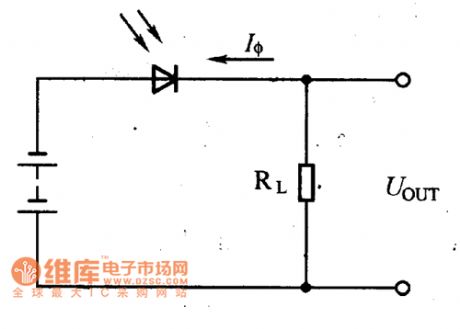
The photosensitive diode is the same as the ordinary photosensitive diode, the PN junction of it has the one-way conductivity, so we need to add the inverse voltage when the photosensitive diode is working, as the figure shows. When there is no illumination, the circuit also has the small reverse saturated leakage current, this is equivalent of the conduction of the photosensitive diode; when there is the illumination, the PN junction is bombarded by the photons, the valence electrons which are bounded absorb the photon energy to produce the electron. The number of these current carriers has little effect for the most of carriers.
Figure:Photosensitive diode principle circuit (View)
View full Circuit Diagram | Comments | Reading(1483)
| Pages:1634/2234 At 2016211622162316241625162616271628162916301631163216331634163516361637163816391640Under 20 |
Circuit Categories
power supply circuit
Amplifier Circuit
Basic Circuit
LED and Light Circuit
Sensor Circuit
Signal Processing
Electrical Equipment Circuit
Control Circuit
Remote Control Circuit
A/D-D/A Converter Circuit
Audio Circuit
Measuring and Test Circuit
Communication Circuit
Computer-Related Circuit
555 Circuit
Automotive Circuit
Repairing Circuit

