power supply circuit
Circuit Diagram of Simplified Voltage Doubler Composed of Inverter
Published:2011/7/2 22:13:00 Author:Vicky | Keyword: Simplified Voltage Doubler | From:SeekIC
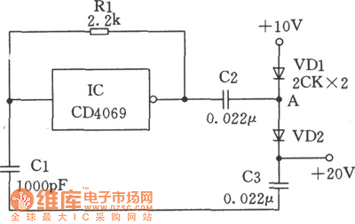
The above picture is a simplest voltage doubler composed of CMOS NOT-Gate CD4069. It is probably the most basic DC/DC booster circuit. 4069, R1 and C1 together constitute a multivibrator of about 100 KHz. The output of the oscillator changes form 0 to 10V. When the output is 0V, the capacitance C2 is charged to 10V via VD1; when the output of oscillator rises to +10V suddenly, because that the two ends of capacitance cannot mutate, end A of capacitance C2 correspondently rises to +20V. Under such circumstance, VDI1 is reverse biased, and the current charges the C3 via VD2, and therefore the output end’s voltage is +20V. However, because there is pressure drop in the diode , the actual output is a litter lower than +20V.
Reprinted Url Of This Article:
http://www.seekic.com/circuit_diagram/Power_Supply_Circuit/Circuit_Diagram_of_Simplified_Voltage_Doubler_Composed_of_Inverter.html
Print this Page | Comments | Reading(3)

Article Categories
power supply circuit
Amplifier Circuit
Basic Circuit
LED and Light Circuit
Sensor Circuit
Signal Processing
Electrical Equipment Circuit
Control Circuit
Remote Control Circuit
A/D-D/A Converter Circuit
Audio Circuit
Measuring and Test Circuit
Communication Circuit
Computer-Related Circuit
555 Circuit
Automotive Circuit
Repairing Circuit
Code: