
Circuit Diagram
Index 1622
Touching dimming delay light circuit
Published:2011/7/1 2:44:00 Author:Ecco | Keyword: Touching , dimming, delay light

Circuit features: as long as touching the film, light will be bright and delay tens of seconds, then the light is not extinguished immediately but gradually darken until turning off. The touch switch has only two pin-out, which can directly replace ordinary light switch without having to change the original wiring. Touching the circuit once, lights can be lit 45 ~ 60s or so, if you want to change the delay time, you can adjust the resistance of resistor R6. R6 resistance is larger, the delay is longer, otherwise shorter.
(View)
View full Circuit Diagram | Comments | Reading(580)
Bedside lamp safety switch circuit (3)
Published:2011/7/1 3:22:00 Author:Ecco | Keyword: Bedside lamp , safety switch
The circuit shown as the chart is bedside lamp safety switch which is composed of batteries and optical coupler, and it can completely isolate bedside switch S and AC, so security is very good.
(View)
View full Circuit Diagram | Comments | Reading(543)
Bedside lamp safety switch circuit (1)
Published:2011/7/1 3:27:00 Author:Ecco | Keyword: Bedside lamp , safety switch
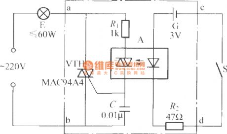
This switch can be directly connected to the power cord of bedside lamp in series, which is easy to use. But after using for a long time, broken power lines will cause accidents, if it uses the safety switch shown as the chart, you can boldly use. Closing switch S, thyristor VT can get the trigger current and open by R1, R2 and S, then the controlled lamp E is lit by geting the normal full-wave alternating current; turning on the switch S, VT will lose the gate trigger current, then light is off as AC is zero crossing.
(View)
View full Circuit Diagram | Comments | Reading(545)
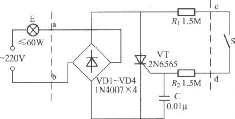
Bed safety dimmer circuit
Published:2011/7/1 3:33:00 Author:Ecco | Keyword: Bed , safety , dimmer

Bed safety dimmer circuit is shown as the chart, and the circuit uses the neon bulb V to couple with the photosensitive resistor RL, high-value resistors R1, R2 to isolate the dimming potentiometer RP from the electric supply phase line, and adjusting RP can change the luminance of light bulb E and turn off the light.
(View)
View full Circuit Diagram | Comments | Reading(791)
Single-switch multiple-light control circuit (3)
Published:2011/7/1 3:16:00 Author:Ecco | Keyword: Single-switch , multiple-light , control
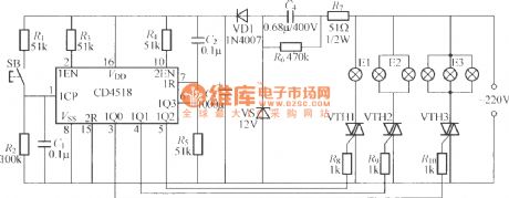
The chart shows the multiple-light circuit which uses single button SB to control, and it can light a group or several groups of groups by the numbers of presssing key, and there is a total of seven states to choose, and the control circuit is suitable for the living room chandelier. VTH1 ~ VTH3 can use MAC94A4 small plastic Triac.
(View)
View full Circuit Diagram | Comments | Reading(787)
Single-switch multiple-light control circuit (2)
Published:2011/7/1 3:04:00 Author:Ecco | Keyword: Single-switch, multiple-light , control

In the circuit shown as the chart, only a power switch S can controll E1, E2 and E3, so it is suitable for the living room chandelier. When S is off, all the lights are off; the first time to connect the S, only the E1 is lit; disconnecting and connecting S in a short time, E1 and E2 are lit; disconnecting and connecting S again, E1 and E3 are lit; disconnecting and connecting S again, all E ~ E3 are lit.
(View)
View full Circuit Diagram | Comments | Reading(868)
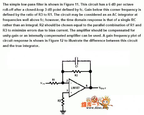
Small low-pass filter circuit
Published:2011/7/4 6:43:00 Author:John | Keyword: low-pass filter
View full Circuit Diagram | Comments | Reading(734)
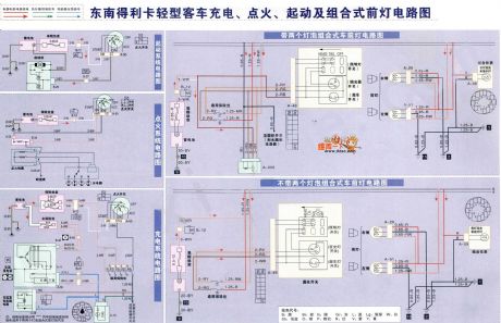
Southeast Delica minibuses charging, ignition, starting and combined headlight circuit
Published:2011/7/4 6:41:00 Author:John | Keyword: minibuses, combined headlight
View full Circuit Diagram | Comments | Reading(817)
QS6K1 internal circuit
Published:2011/7/4 7:20:00 Author:John

View full Circuit Diagram | Comments | Reading(478)
CZX-18-type display power supply circuit
Published:2011/7/4 7:19:00 Author:John | Keyword: display, power supply

View full Circuit Diagram | Comments | Reading(605)
QS6J3 internal circuit
Published:2011/7/4 7:18:00 Author:John

View full Circuit Diagram | Comments | Reading(460)
Monochrome display DARAS CH-5403V-type power supply circuit
Published:2011/7/4 7:17:00 Author:John | Keyword: Monochrome display, power supply

View full Circuit Diagram | Comments | Reading(616)
QS5U26 and QS5U28 internal circuit
Published:2011/7/4 7:07:00 Author:John

View full Circuit Diagram | Comments | Reading(492)
QS6J1 internal circuit
Published:2011/7/4 7:06:00 Author:John

View full Circuit Diagram | Comments | Reading(495)
Logarithmic detection power law circuit
Published:2011/7/4 7:15:00 Author:John | Keyword: detection power law


Logarithmic detector is composed of multi-stage logarithmic amplifiers and its circuit is as shown. A total of five logarithmic amplifiers (A ~ E) are shown in the figure. Gain of each logarithmic amplifier is 20dB (that is five times more of the voltage amplification factor). Its maximum output voltage is limited to 1V. Therefore, the slope value of the logarithmic amplifier is ks = 1V/20dB = 50mV/dB. The output voltage of five pairs of logarithmic amplifier is sent to the summing device (Σ) after respectively though the detector. At the end, the voltage is passing through the low-pass filter to output the voltage Uo. (View)
View full Circuit Diagram | Comments | Reading(764)
Monochrome display DATAS CH-5414 type power supply circuit
Published:2011/7/4 7:06:00 Author:John | Keyword: Monochrome display, power supply

View full Circuit Diagram | Comments | Reading(582)
Temperature-compensated diode input power detector circuit
Published:2011/7/4 7:03:00 Author:John | Keyword: diode, input power detector
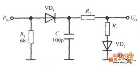
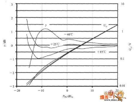
The figure shows the Temperature-compensated diode input power detector circuit. It increases the temperature to compensate the diode VD2 and can compensate temperature to rectified voltage on the diode VD1. Diode has a negative temperature coefficient. When the temperature rises, the pressure drop of the VD1 will reduce, as well as that of VD2. It ultimately remains constant for the output voltage. Compensated Uo, PIN and the error γ of the curve are as shown. The figure also points out the error curve under the ambient temperature of +25 ℃, -40 ℃ and +85 ℃. (View)
View full Circuit Diagram | Comments | Reading(2260)
The 110V regulated power supply cirucit
Published:2011/6/25 5:27:00 Author:Borg | Keyword: regulated, power supply

View full Circuit Diagram | Comments | Reading(633)
HT9215D-The Intergrated PC Dialing Circuit
Published:2011/6/14 23:25:00 Author:Borg | Keyword: Intergrated Circuit, PCs


The HT9215D intergrated circuit of PC dialing is widely used in all kinds of phones.
It is pinned in dual in-line packages with 24 pinnings, whose pin functions and data are listed in Table 1-1.
le
Table 1-1 pin functions and data of HT9215D
(View)
View full Circuit Diagram | Comments | Reading(740)
The emitting circuit composed of SF04E and SF04B
Published:2011/6/25 5:26:00 Author:Borg | Keyword: emitting circuit
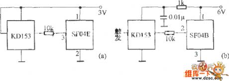
Figure: The emitting circuit composed of SF04E and SF04Ba) indicates the remote emitting circuit composed of SF04E, its coupled reception circuit can be SJ04H components; b) indicates the remote emitting circuit composed of SF04B, which can be coupled as the reception circuit with SJ04E. (View)
View full Circuit Diagram | Comments | Reading(467)
| Pages:1622/2234 At 2016211622162316241625162616271628162916301631163216331634163516361637163816391640Under 20 |
Circuit Categories
power supply circuit
Amplifier Circuit
Basic Circuit
LED and Light Circuit
Sensor Circuit
Signal Processing
Electrical Equipment Circuit
Control Circuit
Remote Control Circuit
A/D-D/A Converter Circuit
Audio Circuit
Measuring and Test Circuit
Communication Circuit
Computer-Related Circuit
555 Circuit
Automotive Circuit
Repairing Circuit