
Circuit Diagram
Index 1632
EW-8W electronic ballast circuit diagram
Published:2011/7/1 1:18:00 Author:Ecco | Keyword: electronic ballast

View full Circuit Diagram | Comments | Reading(2511)
Microwave radar automatic lamp circuit(4)(TWH9250)
Published:2011/7/1 1:14:00 Author:zj | Keyword: Microwave radar automatic lamp circuit(4)(TWH9250), TWH9250, LM7812
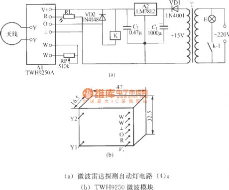
(a) Microwave radar automatic lamp circuit(4)
(b) TWH9250 microwave module
As the diagram shows,the annular antenna can use Φ1~3mm enameled wire to bend to circle andto connect to X,Y ports of the module. (View)
View full Circuit Diagram | Comments | Reading(654)
In-phase addition circuit composed of the LF155
Published:2011/7/3 21:55:00 Author:Rebekka | Keyword: In-phase addition


Themain parameters typical values of the LF155 are:
(View)
View full Circuit Diagram | Comments | Reading(536)
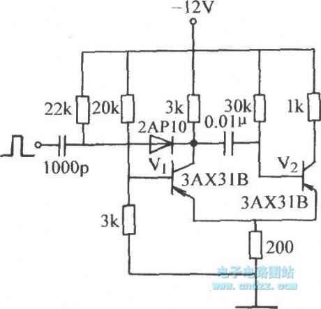
The single key 555 dual steady switch circuit
Published:2011/7/3 20:48:00 Author:Borg | Keyword: single key, dual steady switch
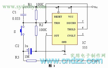
In figure 1 is the circuit. When the circuit gets power, C1 makes 6-pin of IC(555) acquire a positive pulse, the 3-pin is outputting a low LEV, at the moment, there is no voltage on C2. By pressing the key of S, the 0 LEV is working on 2-pin of the IC, 3-pin is reversed in a high LEV, C2 is charged by R3. After S is released, C2 is charged to Vcc, both the 2-pin and 6-pin are offset to 1/2Vcc by R1 and R2, the high LEV of 3-pin remains the same. By pressing S again, the voltage on C2 makes the voltage on 6-pin of the IC higher than 2/3Vcc, and 3-pin is reversed in a low LEV. (View)
View full Circuit Diagram | Comments | Reading(1152)
The single key switch circuit
Published:2011/7/3 20:51:00 Author:Borg | Keyword: single key
View full Circuit Diagram | Comments | Reading(383)
The high speed switch circuit with clamping diodes
Published:2011/7/3 21:19:00 Author:Borg | Keyword: high speed switch, clamping diodes
View full Circuit Diagram | Comments | Reading(584)
The two stage phase inverter circuit with diode protection
Published:2011/7/3 20:54:00 Author:Borg | Keyword: phase inverter, diode protection
View full Circuit Diagram | Comments | Reading(597)
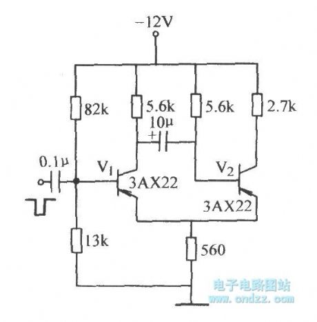
The starting circuit of single steady state
Published:2011/7/3 20:56:00 Author:Borg | Keyword: starting circuit, single steady state
View full Circuit Diagram | Comments | Reading(504)
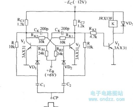
The dual steady circuit with relays
Published:2011/7/3 20:57:00 Author:Borg | Keyword: steady circuit
View full Circuit Diagram | Comments | Reading(471)
The circuit of the phase inverter with lamps
Published:2011/7/3 20:59:00 Author:Borg | Keyword: phase inverter
View full Circuit Diagram | Comments | Reading(482)
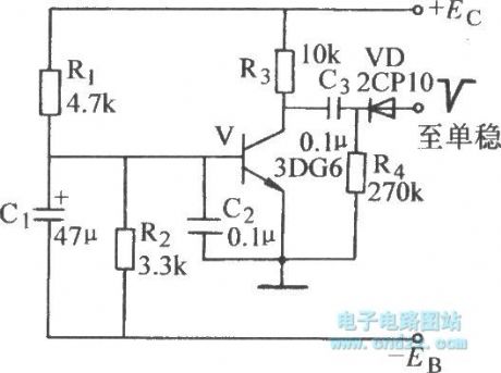
The single steady circuit with trigger signals on the basic pole of blanking tubes
Published:2011/7/3 21:18:00 Author:Borg | Keyword: single steady circuit, trigger signals, basic pole
View full Circuit Diagram | Comments | Reading(491)
The single steady circuit with trigger signals on the basic pole of the conducting pipe
Published:2011/7/3 22:01:00 Author:Borg | Keyword: single steady circuit, trigger signals, conducting pipe
View full Circuit Diagram | Comments | Reading(450)
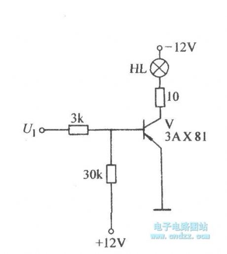
The touching switch circuit
Published:2011/7/3 21:20:00 Author:Borg | Keyword: touching switch

View full Circuit Diagram | Comments | Reading(519)
The touching interlock electric switch circuit
Published:2011/7/3 21:32:00 Author:Borg | Keyword: interlock, electric switch


Usually, the RC of the phase inverter input terminal makes the output terminal 0, when touching the line i (i=0,1,2```7), the signal that is inducted by human body is sent to Di terminal and CLK terminal of 74LS374 respectively, at the moment, the CLK has the rising cause, so the state of D (except Di=1, others are 0) is locked on the Q terminal(Qi=Di=1), the corresponding LED is glowing; when the signal is gone(means no touch), the circuit is reset, so CLK has no rising cause.Therefore, only one line of lights are glowing when only one line is touched, which can fulfill the aim of interlocking and indication. (View)
View full Circuit Diagram | Comments | Reading(587)
The mains over-voltage protection circuit of excellent nature
Published:2011/7/3 21:55:00 Author:Borg | Keyword: over-voltage protection, mains

See as the figure, the circuit adopts the capacitor step-down and the simple regulated power supply circuit, when the power supply is normal, the voltage controlled by TL431C is lower than 2.5V, and TL431C is blocked, the relay is open. When the mains voltage is higher than 250V, the current which has been rectified and filtered reaches 3.3mA, the voltage drops on R3, diode and stabilivolt (including glow tube) are 11v and 26v, respectively. The 37V voltage is distributed by R1 and R2, the voltage on the distributing point is 2.55v, TL431C is conducting, the relay is pulling in, the mains is short, which make the current protector jump or the fuse blow out.
(View)
View full Circuit Diagram | Comments | Reading(1714)
The wide band AC separation amplifier circuit of photoelectric couplers
Published:2011/7/3 22:11:00 Author:Borg | Keyword: wide band, AC separation amplifier, photoelectric couplers

In th figure is the wide band AC separation amplifier circuit of photoelectric couplers. When there's no modulation, the photoelectric coupler must work with a DC bias current which is offered by VT1, VD1 is used to improve the temperature feature of VT1. In the circuit, the 6N136 photoelectric coupler is adopted, the LED of it outputs a very low current which is amplified by the transistor. To improve the frequency feature, the common pole circuit composed of TV2 converts the current into the voltage. The voltage gain is decided by the resistor R2 on the collecting electrode of VT2, the working point adjustment is decided by R1.
(View)
View full Circuit Diagram | Comments | Reading(773)
The HCS301 encoder application circuit in wireless emitting circuits
Published:2011/7/3 22:23:00 Author:Borg | Keyword: encoder, wireless emitting circuits
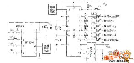
HCS301 rolling encoder chip is developed on the base of non-linear flow code algorithm, which includes the 66-bit transmitting code, 32-bit rolling code, 64-bit programmable secrete key, 32-bit source code, which can generates 266 kinds of combination, which can make sure that the codes won't repeat in 18 years. The special algorithm can make the rolling decoder only react to a code once in the valid period, and every code is sent randomly, the decoding is impossible. The HCS301 encoder circuit, which is applied in wireless emitting circuits, is shown in the figure.
(View)
View full Circuit Diagram | Comments | Reading(4376)
The singal terminal (A) power amplifier circuit of ultra 3-pole valve connection
Published:2011/7/3 22:25:00 Author:Borg | Keyword: singal terminal, power amplifier, valve connection

The singal terminal (A) power amplifier circuit of ultra 3-pole valve connection is shown as above.
(View)
View full Circuit Diagram | Comments | Reading(600)
The FM l2 wave band radio circuit of Desheng ll9700
Published:2011/7/3 22:28:00 Author:Borg | Keyword: wave band, Desheng

The FM l2 wave band radio circuit of Desheng ll9700 is shown as above.
(View)
View full Circuit Diagram | Comments | Reading(1318)
The inductance controlled switch circuit (3)
Published:2011/7/2 23:08:00 Author:Borg | Keyword: inductance controlled, switch circuit

The circuit that will be introduced can be used to control the lighting lamp and auto door, and it can also be used to burglarproof alarm. This circuit consists of the inducting electrode plate A, regulated diode VS, FET transistor VF, music integrated circuit IC, transistor V, relay K, diode VD, resistor R1 and R2, potentiometer RP and power supply switch S, etc, see as the figure.
The inductance controlled switch circuit By adjusting the potentiometer RP, the music time of the IC can be changed, so the working time of the load can be changed. (View)
View full Circuit Diagram | Comments | Reading(509)
| Pages:1632/2234 At 2016211622162316241625162616271628162916301631163216331634163516361637163816391640Under 20 |
Circuit Categories
power supply circuit
Amplifier Circuit
Basic Circuit
LED and Light Circuit
Sensor Circuit
Signal Processing
Electrical Equipment Circuit
Control Circuit
Remote Control Circuit
A/D-D/A Converter Circuit
Audio Circuit
Measuring and Test Circuit
Communication Circuit
Computer-Related Circuit
555 Circuit
Automotive Circuit
Repairing Circuit