
Circuit Diagram
Index 1629
Tcc series silicon violet-blue battery circuit
Published:2011/7/4 4:03:00 Author:Christina | Keyword: Tcc series, silicon, violet-blue battery

Tcc series silicon violet-blue battery circuit
(View)
View full Circuit Diagram | Comments | Reading(527)
Photosensitive alarm circuit
Published:2011/7/4 4:01:00 Author:Christina | Keyword: Photosensitive alarm
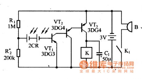
The photosensitive alarm circuit is as shown in the figure. The R1 and R2 are the partial voltage bias circuits. When there is no illumination, the silicon photocell will not produce the voltage, it only the resistance which is connected in the base circuit of the amplifier. When there is the illumination, the silicon photocell will produce the voltage, this voltage and the ground voltage add to the base electrode of VT1 together, so the VT1, VT2 and VT3 conduct, the relay K starts working, the contact point closes, the buzzer sends out the alarm.
This alarm circuit can be used in the anti-theft alarm of the drawer cabinet.
Figure:Photosensitive alarm circuit (View)
View full Circuit Diagram | Comments | Reading(515)
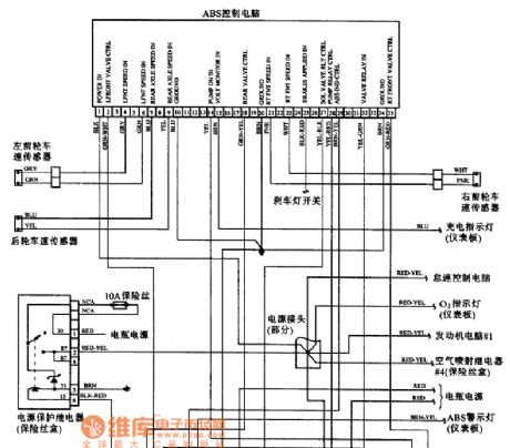
BENZ 190 series ABS system circuit
Published:2011/7/4 3:44:00 Author:Christina | Keyword: BENZ, ABS, system circuit
BENZ 190 series ABS system circuit (View)
View full Circuit Diagram | Comments | Reading(608)
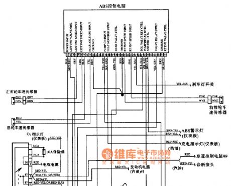
BENZ 300SDL, 420, 560DEL and 560SEC ABS system circuits
Published:2011/7/4 3:36:00 Author:Christina | Keyword: BENZ, ABS system
BENZ 300SDL, 420, 560DEL and 560SEC ABS system circuits
(View)
View full Circuit Diagram | Comments | Reading(435)
Vehicle circuit with the 8-pin diagnosis connector
Published:2011/7/4 1:57:00 Author:Christina | Keyword: Vehicle circuit, 8-pin, diagnosis connector
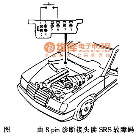
Vehicle circuit with the 8-pin diagnosis connector
(View)
View full Circuit Diagram | Comments | Reading(442)
Transistor radio application circuit of the ceramic filter
Published:2011/7/4 1:38:00 Author:Christina | Keyword: Transistor radio, application circuit, ceramic filter
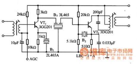
The transistor radio application circuit of the two-port and three-port ceramic filter. The ceramic filters B1 and B2 can be used in the 465kHz intermediate frequency bypass, the B1 can be used in the coupling of the intermediate frequency. B1 uses the narrowband type filter, and it is connected with the emitter resistance of the VT1, this design helps to eliminate the interference and noise.
Figure 1 The transistor radio application circuit of the ceramic filter
(View)
View full Circuit Diagram | Comments | Reading(1495)
Light metering stationery case light metering circuit
Published:2011/7/4 1:01:00 Author:Christina | Keyword: Light metering, stationery case, light metering circuit

The light metering circuit of the light metering stationery case is as shown in the figure. This circuit uses the 2CRll silicon photocell as the light metering component, and this 2CRll silicon photocell is installed on the surface of the stationery case to feel the light intensity. The VD1 and VD2 are two light-emitting diodes that can be used to indicate the strength of the light. When the illumination is less than 10Olx, the voltage which is produced by the silicon photocell is small, the VT1's tube voltage is large or it is in the cut-off state, the two light-emitting diodes VD1 and VD2 will not turn on; when the illumination is between 100-20Olx, the voltage that is produced by the silicon photocell will increases, the voltage drop of VT1 reduces, the light-emitting diode VD2 turns on, this means the illumination is moderate.
(View)
View full Circuit Diagram | Comments | Reading(537)
Two-way thyristor AC voltage regulation circuit
Published:2011/7/4 1:31:00 Author:Christina | Keyword: Two-way thyristor, AC, voltage regulation
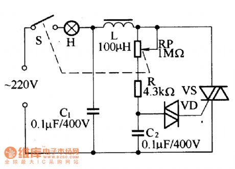
The two-way thyristor AC voltage regulation circuit is as shown in the figure. Because the thyristor is working in the AC circuit, both of the positive and negative phases can be conductd, so the main circuit is more simple than the unidirectional thyristor regulation circuit. Also you can change the conduction angle to achieve the purpose of regulating.
The light regulation desk lamp circuit which uses the two-way thyristor is as shown in the figure. When the switch S closes, the AC city electricity charges the capacitance C2 through the incandescent bulb, L, RP and R. When the voltage of C2 increases to the conduction voltage of the bi-polar tube, the VD conducts to trigger the two-way thyristor to conduct.
(View)
View full Circuit Diagram | Comments | Reading(1543)
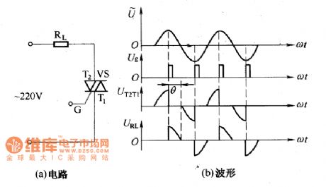
Unidirectional thyristor AC voltage regulation circuit
Published:2011/7/4 1:18:00 Author:Christina | Keyword: Unidirectional thyristor, AC, voltage regulation
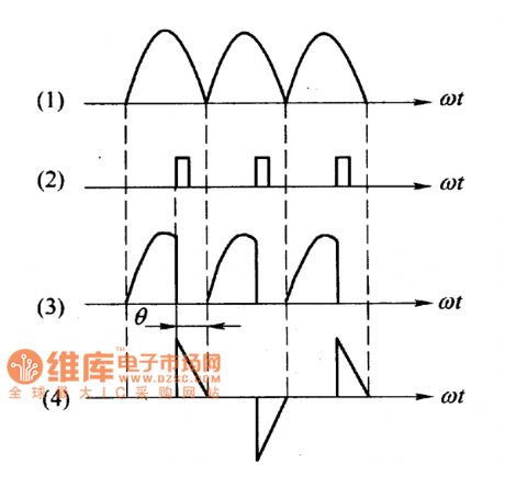
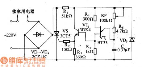
The unidirectional thyristor AC voltage regulation circuit is as shown in the figure a. The load RL is connected in the AC return circuit, the current which flows through it is controlled by the unidirectional thyristor VS's conduction and cut-off. The AC voltage is rectified and is changed into the unidirectional pulsating voltage UAK, as the figure (1) shows. You can change the AC voltage effective value of load Rl by changing the unidirectional thyristor conduction angle θ to achieve the purpose of alternating voltage regulation.
Figure (b) shows one kind of household appliances pressure regulating device, it can be used in the thermoregulation of the electric blanket and the electric iron, also it can be used in the dimming of the table light.
(View)
View full Circuit Diagram | Comments | Reading(1108)
MG type photosensitive resistor dimension circuit
Published:2011/7/4 19:36:00 Author:Christina | Keyword: MG type, photosensitive resistor, dimension circuit
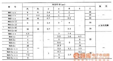
Table: MG type photosensitive resistor dimensions (View)
View full Circuit Diagram | Comments | Reading(536)
Unijunction transistor sawtooth wave generator circuit
Published:2011/7/4 19:34:00 Author:Christina | Keyword: Unijunction transistor, sawtooth wave, generator circuit
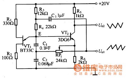
The sawtooth wave generator circuit is as shown in figure 1. It uses the unijunction transistor multivibrator as the foundation, and it has a emitter follower. It can produce the positive and negative sawtooth wave voltage which has good linearity.
Figure 1 The sawtooth wave generator circuit principle diagram
(View)
View full Circuit Diagram | Comments | Reading(1472)
Unijunction transistor delay circuit
Published:2011/7/4 19:30:00 Author:Christina | Keyword: Unijunction transistor, delay circuit
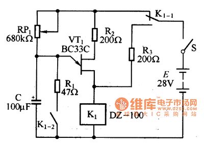
The delay circuit which is composed of the unijunction transistor is as shown in figure 1. When the power supply is connected, the +28V power adds to the unijunction transistor delay circuit through the normally closed contact point of the conversion contact point K1-1 of the relay K1, so the delay circuit starts working. The capacitance C is charged through RP1, when the charging voltage Vc of the C is the same as the peak voltage of the unijunction transistor, the VT conducts, the C discharges through VT and K1, so the discharging current is large, the relay K closes, the normally open contact point of the conversion contact point K1-1 closes, and the normally closed contact point cuts off, the power of the timing circuit turns off.
Figure 1 The delay circuit
(View)
View full Circuit Diagram | Comments | Reading(1146)
Unijunction crystal thyristor trigger circuit
Published:2011/7/4 19:21:00 Author:Christina | Keyword: Unijunction crystal, thyristor, trigger

The thyristor trigger circuit is as shown in figure 1. The unijunction crystal thyristor forms the self-excited multivibrator, the series pulse current which is produced by it flows through the pulse transformer T, so the secondary stage of the transformer T will produce a series of pulse voltage, the VD1 cuts the negative pulse of this series pulse and this pulse adds to the triggered thyristors VS between the control electrode and the cathode.
The pulse transformer of this circuit can be used to trigger the pulse generating circuit and isolate the thyristor main circuit.
Figure 1 The thyristor trigger circuit
(View)
View full Circuit Diagram | Comments | Reading(1322)
Light control flashing warning light circuit
Published:2011/7/4 7:32:00 Author:Christina | Keyword: Light control, flashing, warning light
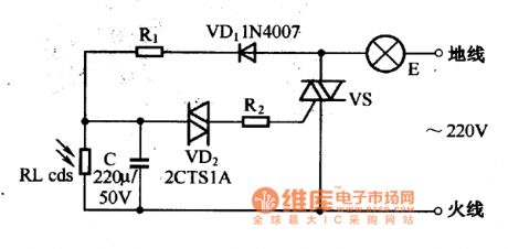
The light control flashing warning light will automaticly turn off, and at night ,the light will automaticly turn on.
The light control flashing warning light circuit is as shown in the figure. When the power is connected, the 220V city electricity will be half wave rectified by the diode VD1, and it charges the C through R1, so the charging current is small, the warning light E will not turn on. The voltage of capacitance C depends on the R1 and the partial voltage value of the photoconductive resistance RL.
In the day time, the photoconductive resistance RL is illuminated by the natural light source, so it has the low resistance, the charging voltage of the capacitance C will not exceed the turning voltage of the two-way trigger diode VD.
Light control flashing warning light circuit (View)
View full Circuit Diagram | Comments | Reading(646)
Sound control photosensitive delay switch circuit
Published:2011/7/4 6:40:00 Author:Christina | Keyword: Sound control, photosensitive, delay, switch circuit

Figure:Sound control photosensitive delay switch circuit
The sound control photosensitive delay switch circuit is as shown in the figure. In the daytime, the photoconductive resistance RL is irradiated by the light, so it is in the low impedance state to conduct the semiconductor tube VT3, so the VT4 and VT5 cut off, the VT6 conducts, the thyristor VS cuts off, the bulb E is in the off state. Because the VT3 is in the conduction state, so no matter what the sound is, the bulb E will not turn on.
At night ,there is no light, so the photoconductive resistance's internal resistance increases to make the VT3 in the cut-off state. If there is no sound, the circuit is the same as the circuit of the daytime; when there is the sound, the microphone B receives the sound signal and changes it into the electrical signal. (View)
View full Circuit Diagram | Comments | Reading(915)
2CR series rectangular silicon photocell appearance circuit
Published:2011/7/4 6:30:00 Author:Christina | Keyword: 2CR series, rectangular, silicon photocell, appearance circuit

2CR series rectangular silicon photocell appearance circuit
(View)
View full Circuit Diagram | Comments | Reading(564)
2CR series rounded silicon photocell appearance circuit
Published:2011/7/4 6:29:00 Author:Christina | Keyword: 2CR series, rounded, silicon photocell, appearance circuit

2CR series rounded silicon photocell appearance circuit
(View)
View full Circuit Diagram | Comments | Reading(507)
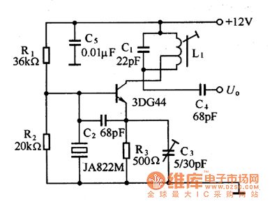
27MHz quartz crystal oscillator circuit
Published:2011/7/4 6:27:00 Author:Christina | Keyword: 27MHz, quartz crystal, oscillator circuit

The 27MHz quartz crystal oscillator circuit is as shown in figure 1. The biasing circuit is composed of the R1, R2 and R3, C6 is the bypass capacitor. The partial voltage circuit is composed of the C1, C2, C3 and C4 to control the strength of oscillation. L1 is the high-frequency choke coil, it has the role of filtering.
Figure 1 The 27MHz quartz crystal oscillator circuit
The quartz crystal resonator JAl2B is in the parallel resonant state, the oscillation frequency of the oscillator depends on the natural frequency of the crystal. The L2 and C5 determine the oscillation strength. (View)
View full Circuit Diagram | Comments | Reading(3454)
Tcc series silicon photocell appearance circuit
Published:2011/7/4 6:09:00 Author:Christina | Keyword: Tcc series, silicon photocell, appearance circuit

Tcc series silicon photocell appearance circuit
(View)
View full Circuit Diagram | Comments | Reading(687)
44MHz quartz crystal oscillator circuit
Published:2011/7/4 6:20:00 Author:Christina | Keyword: 44MHz, quartz crystal, oscillator
The 44MHz quartz crystal oscillator circuit is as shown in figure 1. In order to get the high oscillation frequency, this circuit uses the frequency multiplication oscillation circuit. The L1 and C1 tune at 44MHz, the fundamental wave 22MHz is mistermination, so this is the short-circuit. The quartz crystal resonator uses the 22MHz resonator, it has the sensibility in the circuit, the partial voltage capacitance are C2 and C3. For the 22MHZ fundamental wave, the circuit is the three-point capacitance oscillation circuit, you can get the 22MHz oscillation signal from the emitter.
Figure 1 The 44MHz quartz crystal oscillator circuit
(View)
View full Circuit Diagram | Comments | Reading(756)
| Pages:1629/2234 At 2016211622162316241625162616271628162916301631163216331634163516361637163816391640Under 20 |
Circuit Categories
power supply circuit
Amplifier Circuit
Basic Circuit
LED and Light Circuit
Sensor Circuit
Signal Processing
Electrical Equipment Circuit
Control Circuit
Remote Control Circuit
A/D-D/A Converter Circuit
Audio Circuit
Measuring and Test Circuit
Communication Circuit
Computer-Related Circuit
555 Circuit
Automotive Circuit
Repairing Circuit