
Circuit Diagram
Index 495
5V Current Limiter Composed Of MIC2951 Circuit
Published:2011/9/6 4:48:00 Author:Felicity | Keyword: 5V, Current Limiter

View full Circuit Diagram | Comments | Reading(831)
Application Circuit of LCD TV Power
Published:2011/9/3 10:19:00 Author:Zoey | Keyword: Application Circuit, LCD TV Power
PLC810PG group and LLC lineless controller integrate with high pressure half-bridge driver. Picture 1 shows the circuit of PLC810PC power supply configuration.
PFC of PLC810PG uses a general continuous current mode that does not have to refer to sine signal, in this way, costs of the system and exterior accessories are reduced.
DC-DC controller drives the LLC resonance topologies.
Dead band time of LLC switch in PLC810PG can be adjusted by an exterior resistance.
PFC converter’s frequency is limited in LLC to reduce the interference of noise and electromagnetism.
This design also refers to elementary exception handles of PFC and LLC. Dynamic adjustment can be achieved by consulting phase proportion of LLC to PFC.
(View)
View full Circuit Diagram | Comments | Reading(1095)
High-precision Constant Current Source Circuit Consisting of TL431
Published:2011/9/3 10:20:00 Author:Zoey | Keyword: High-precision, Constant Current Source
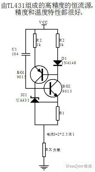
High-precision constant current source circuit consisting of TL431 has an excellent precision and temperature characteristics. (View)
View full Circuit Diagram | Comments | Reading(9993)
Low-end Car Charger Circuit Diagram Achieved by Single Chip 34063
Published:2011/9/3 10:13:00 Author:Zoey | Keyword: Low-end, Car Charger, Single Chip 34063
Advantage: Low cost
Disadvantage:
(1) Undesirable reliability, single performance, no overtemperature and short circuit-proof measures.
(2) Inputs direct current voltage, but controls input constant charge current by limiting maximum switched current peak, its precision is not accurate enough.
(3) As 34063 belongs to a 1.5-A switched current PWM+PFM mode (no interior error magnifier), its automobile charge inputs relatively larger wave of direct voltage and current, the wave is not pure enough and its ability to input current is limited. (often been seen in low-end automobile charge ranging from 300 ma to 600 ma) (View)
View full Circuit Diagram | Comments | Reading(799)
Pulse Charge Time Relay Circuit
Published:2011/9/3 10:03:00 Author:Zoey | Keyword: Pulse Charge, Time Relay
Pulse Charge Time Relay Circuit (View)
View full Circuit Diagram | Comments | Reading(923)
FET Time Relay Circuit
Published:2011/9/3 10:01:00 Author:Zoey | Keyword: FET, Time Relay
FET Time Relay Circuit (View)
View full Circuit Diagram | Comments | Reading(960)
A High Power Drive Circuit without an Exterior Switch
Published:2011/9/3 10:00:00 Author:Zoey | Keyword: High Power Drive, LED Circuit, Exterior Switch
High power LED, candescence light bulb and fluorescence lamp are widely used for illumination. Current source is the best way to offer LED power. As to the LEDs that have a current larger than 0.35A, induction switched voltage regulator is the best matcher.
This design solution offers a series of circuits for single power integrated circuit regulators, so as to improve efficiency and reduce the size.
Circuit in picture 1,2 and 3 adopt circuit that is composed of three or four alkalescence cells, NiMH cells or NiCd cells for power supply. Circuits in picture 4 and 5 can be used in automobiles, industry systems and emergency branch systems and telecoms, the circuits’ circuitry voltage of switch system is 12V, 24V or 42V.
When the circuits begin to work, they will darkle. Resistances and potentiometers can get power by VD or CVL terminal of the interior voltage regulator.
(View)
View full Circuit Diagram | Comments | Reading(819)
Voltage Three-phase Bridge and Push-pull Inverter Circuit
Published:2011/9/3 9:17:00 Author:Zoey | Keyword: Voltage, Three-phase, Bridge, Push-pull, Inverter Circuit
Voltage three-phase bridge and push-pull inverter circuit
In addition to the inverter output waveform performanceindex, Performance indicators should also include: Inverter efficiencyPower output bya unitofweight (or volume)Reliability index AC component value and pulse frequency of DC current input by the inverterElectromagnetic interference (EMI) and electromagnetic compatibility EMC Push-pull single-phase inverter circuit (View)
View full Circuit Diagram | Comments | Reading(1495)
The digital paging systems F36-F and F36-J
Published:2011/9/4 20:33:00 Author:TaoXi | Keyword: Digital paging system
The transmission circuit:
The receiving circuit:
(View)
View full Circuit Diagram | Comments | Reading(910)
The digital telemetering thermometers FDD5 and JDD5
Published:2011/9/4 20:34:00 Author:TaoXi | Keyword: Digital telemetering thermometer
Transmitter circuit:
The temperature detecting circuit is composed of the temperature integrated sensor AD590, this circuit changes the temperature variation into the output current variation. AD590's output current is proportional to the measurement temperature, as the temperature increases, the output current increases with the 1μA/K constant ratio. When the output current gets through RP2, at the top of RP2 forms the voltage, and this voltage is amplified by the voltage amplifier and is used as the voltage-frequency changer's control voltage.
Receiving circuit:
(View)
View full Circuit Diagram | Comments | Reading(1009)
A Circuit Diagram of Discrete Elements of the Touch Switch
Published:2011/9/3 20:08:00 Author:Zoey | Keyword: Circuit Diagram, Discrete Elements, Touch Switch
The circuit of discrete elements of the touch switch has been shown in picture below. This circuit is composed of an induction magnifier, a memorizer and an AC driver. As soon as a finger touches the insulted plate, a small AC signal will be added to the gate of Tr1, the signal will produce square wave on R4 after being magnified, and then it will charge to C3 through Tr3, after that it will produce direct input voltage on R8, the voltage will be added to single crystal transistor Tr6. Finally, Tr6 will give rise to remittent oscillation and trigger the controllable silicon. The longer the switch is touched, the larger of voltage on R8 will be. As soon as the finger leaves the switch, load will be cut off. (View)
View full Circuit Diagram | Comments | Reading(1037)
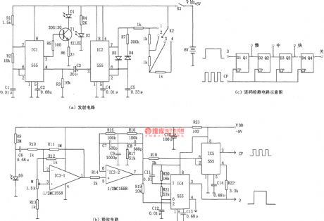
The infrared remote control dimmer switch circuit KA2184A
Published:2011/9/4 20:34:00 Author:TaoXi | Keyword: Infrared, remote control, dimmer switch
The circuit is as shown in the figure. It includes the infrared emission circuit, the infrared receiver circuit, the decoder circuit, the dimming control circuit and the birds voice circuit.etc. You can use this circuit to achieve the remote control switching and dimming of the wall lamp, droplight, the remote control distance is more than 7m, and it is easy to operate and has reliable performance.
Infrared emission circuit:
Oscillation frequency:
Infrared receiving control circuit:
(View)
View full Circuit Diagram | Comments | Reading(1051)
The infrared remote control music socket circuit 3
Published:2011/9/4 20:35:00 Author:TaoXi | Keyword: Infrared remote control, music socket
The circuit is as shown in the figure. It includes the infrared remote transmitter circuit, the decoder circuit, the relay control circuit and the music circuit.etc. The infrared pulse transmitter circuit is composed of the 25kHz pulse oscillation circuit and the external transmitter driver circuit. And the 25kHz pulse oscillator is composed of the F1, F 2 and R1, R2, C1 components which belong to the Six NAND gate IC CD4069.
Infrared transmitter circuit:
Infrared receiver and control circuit:
(View)
View full Circuit Diagram | Comments | Reading(921)
Single stage power factor dimming type fluorescent lamp electronic ballast design
Published:2011/9/4 20:39:00 Author:TaoXi | Keyword: Single stage, power factor, dimming type, fluorescent lamp, electronic ballast design


The frequency control means to change the fs switching frequency, so the operating frequency is away from the natural resonant frequency of the resonant network to reduce the lamp power, at this time, the duty cycle D is constantly. The duty cycle modulation means that when the fs is constantly, you change the conduction time of the switch, the reduction of the conduction time reduces the energy that is delivered to the lamp, so the power of the light reduces. The duty cycle modulation range is from 0 to 0.5, so it limits the dimming range. The DC bus voltage regulation means that you can change the amplitude value of the DC bus voltage, and keep the fs and D unchanged.
(View)
View full Circuit Diagram | Comments | Reading(736)
The practical nickel cadmium battery automatic charger circuit
Published:2011/9/4 20:40:00 Author:TaoXi | Keyword: Practical nickel cadmium battery, automatic charger

The charge which is introduced in this article can supply the stable charging current and it has the timing circuit to control the charging time.
As the figure 4-17 shows, when youpress the button SW1, the city electricity is connected, the relay RL1 closes, the red light emitting diode LED2 turns on, this means that the charger has connected with the power. The regulator IC5 supplies the 12V DC voltage to the RL1. The regulator IC2 supplies the +5V voltage to the logic circuit. The constant current source is composed of IC1, it can output the stable charging current. R1 fixes the charging current at 50mA (used to charge the LR06 type storage battery), R6 fixes the charging current at 11mA (used to charge the 9V 6F22 type laminated battery).
(View)
View full Circuit Diagram | Comments | Reading(860)
Large power adjustable charger circuit
Published:2011/9/4 20:41:00 Author:TaoXi | Keyword: Large power, adjustable, charger, circuit

The principle of this charging device is as shown in figure 3-7, the maximum output current is 20A, the highest charging voltage is 80V. It can be adjusted from 0V, so it can charge all kinds of batteries and the battery groups or battery groups in series which have the same specifications, such as five 12V batteries in series. By charging the series batteries, we can shorten the length of wiring and reduce the power consumption, so the operating efficiency is improved.
(View)
View full Circuit Diagram | Comments | Reading(884)
Zhonghua saloon car ABS circuit (3)
Published:2011/9/4 20:43:00 Author:TaoXi | Keyword: ZhongHua, saloon car, ABS

The ZhongHua saloon car ABS circuit (3)
D08-grounding L3-brake shoe attrition indicator light S05-Left front wheel brake shoe attrition sensor S06-Right front wheel brake shoe attrition sensor T5-Engine room right wiring harness and dashboard connector T15-Engine room left wiring harness and dashboard connector T16-dashboard wiring harness and integrated instrument panel plug-in connector U37PA-connection point, in the dashboard wiring harness (View)
View full Circuit Diagram | Comments | Reading(788)
High speed switching circuit composed of the SW-239
Published:2011/9/4 20:44:00 Author:TaoXi | Keyword: High speed, switching circuit

The High speed switching circuit composed of the SW-239 is as shown in the figure. This kind of circuit uses the high speed switch SW-239, and it switches the pathes of a few MHZ to several hundred megahertz high frequency signals. The switching speed is decided by the optocoupler PC9DlO. The SW-239 has the 50Ω resistance, the RFcircuit isalways in the open-circuit state before and after the switching, so it has very low coupling to the switch and the surround circuit, the switch conduction and the deadline isolation degree are very high. So when the circuit is switching, it will not produce the peak voltage pulse. RP1 can be used to adjust the gain (before and after the switching).
(View)
View full Circuit Diagram | Comments | Reading(1740)
Multi-functional infrared remote controller 555, MC1558
Published:2011/9/4 20:45:00 Author:TaoXi | Keyword: Multi-functional, infrared, remote controller
The multi-functional infrared remote controller is as shown in the figure. This circuit is composed of the infrared pulse launch circuit and the infrared receiving circuit. The infrared transmitter is as shown in figure (a), it is composed of two multivibrators which use the time-base circuit 555 as the core. The oscillation frequency of the multivibrator which is composed of the IC1(555) and R1, R2, C1 is f=1.44/(R1+2R2)C1, the corresponding frequency of the parameters in the figure is about 3kHz, the signal can be used to drive the carrier wave of the infrared emission diode D1. Another multivibrator is composed of the IC2(555), C5, R7 and the resistor which is connected with the switch K2, it can be used in the keying coding application. The output pulse waveform adds to the pin-4 of IC1 that can be used as the keying modulation signal.
(View)
View full Circuit Diagram | Comments | Reading(1887)
BAX type tone control circuit
Published:2011/9/4 20:45:00 Author:TaoXi | Keyword: BAX, tone control

The BAX type tone control circuit is as shown in the figure. This kind of circuit has low output impedance and input impedance, if the prestate output impedance is not lower enough, you can not get the desired characteristics. The control potentiometer need to use the B-type potentiometer.
(View)
View full Circuit Diagram | Comments | Reading(1455)
| Pages:495/2234 At 20481482483484485486487488489490491492493494495496497498499500Under 20 |
Circuit Categories
power supply circuit
Amplifier Circuit
Basic Circuit
LED and Light Circuit
Sensor Circuit
Signal Processing
Electrical Equipment Circuit
Control Circuit
Remote Control Circuit
A/D-D/A Converter Circuit
Audio Circuit
Measuring and Test Circuit
Communication Circuit
Computer-Related Circuit
555 Circuit
Automotive Circuit
Repairing Circuit