
Circuit Diagram
Index 498
The regulator: DC-DC circuit, power supply monitor pin and its main features LM199A/299A/399A
Published:2011/8/30 2:28:00 Author:Seven | Keyword: DC-DC circuit, power supply, monitor pin

LM199A/299A/399A reference voltage circuit This a reference voltage circuit of high precision, low temperature drift and low noise; its output voltage is 6.95v; output voltage fault is ±2%(but LM399A); LM199A/299A temperature drift is 0.00005%/℃, and that of LM399A is 0.0001%/℃; its working current range is 0.5~10mA; its working impedance typical value is 0.5Ω; the typical value of long-term stability is 20*10-6/1000h; its inverting current is 10mA; the working temperature is LM199A is -55~+125℃, LM299A is -25~+85℃, LM399A is 0~+70℃.
(View)
View full Circuit Diagram | Comments | Reading(731)
The regulator: DC-DC circuit, power supply monitor pin and main features LM185-2.5/285-2.5/385-2.5
Published:2011/8/30 2:29:00 Author:Seven | Keyword: DC-DC circuit, power supply, monitor pin
LM185-2.5/285-2.5/385-2.5 reference voltage circuit (+2.5V) This is a 2-terminal high-voltage circuit of high precision, low temperature drift and low noise; the output voltage is +2.5V; LM185-2.5/285-2.5 output voltage fault is ±1.5%, LM385-2.5 is ±3%; its working current range 20μA~20mA; temperature drift is 20*10-6/℃; the long-term time stability is 20*10-6/1000h; the maximum reversed current is 30mA; the maximum forward current is 10mA; LM185-2.5 working temperature is -55~+125℃, LM285-2.5 is -25~+85℃ and LM385-2.5 is 0~+70℃.
(View)
View full Circuit Diagram | Comments | Reading(643)
The regulator: DC-DC circuit, power supply monitor pin and its main features LM185/285/385
Published:2011/9/5 22:51:00 Author:Seven | Keyword: DC-DC circuit, power supply, monitor pin

LM185/285/385--the Vref circuitThis is a high-precision, low-temperature drift and low-noise circuit which allows no Vref diodes on its 2 terminals; the output voltage range is 1.24~5.30V; the output voltage fault is ±1%(B series); the working current range is 10μA~20mA; the typical value of working impedance is 1Ω; the max reversed current is 30mA; the max forward current is 10mA; the working temperature of LM185 is -55~+258℃, LM285 IS -55~+258℃ and LM385 is 0~+70℃.
(View)
View full Circuit Diagram | Comments | Reading(741)
The regulator: DC-DC circuit, power supply monitor pin and its main features LM140LA/340LA
Published:2011/8/24 21:52:00 Author:Seven | Keyword: DC-DC circuit, power supply, monitor pin

LM140LA/340LA--the 3-terminal stabilizer (forward output) This is a 3-terminal stabilizer with fixed output voltage; its output voltage can be 5V, 12v and 15V; its output current is 100mA; its input stability is 0.04%/V; its load stability is 0.01%/mA; its max input voltage is 35V; the working temperature of LM140LA is +55~+125℃ and that of LM340LA is 0~+70℃; it contains the current limitation, overheat cutoff and sate working area protection circuit; LM140LA is in metal package, LM340LA is in either metal or plastic package.
(View)
View full Circuit Diagram | Comments | Reading(793)
The regulator: DC-DC circuit, power supply monitor pin and its main features LM1578/2578/3578
Published:2011/9/5 22:52:00 Author:Seven | Keyword: DC-DC circuit, power supply, monitor pin

LM1578/2578/3578--the switch stabilizer control circuitThis is a DC-DC converter control circuit; it consists of the comparator, reference power supply, oscillating circuit and switch transistor; it can compose the booster, step-down and phase inverting circuit; the working power supply voltage range is 2~40V; the switch current is 750mA; the oscillating frequency can be set as 100kHz; the duty cycle period range is 0~90%; the voltage difference range between the electrode of the switch transistor (C terminal) and the earth is -0.3~+40V and that of the switch transistor emitter (E terminal) and the ground is -1~+40V.
(View)
View full Circuit Diagram | Comments | Reading(788)
The regulator: DC-DC circuit and power supply monitor pin and its main features DS2437S
Published:2011/8/30 2:29:00 Author:Seven | Keyword: regulator, power supply, monitor pin

DS2437S—the intelligent cell monitorOnly one pin is for communication; each componenthas a unique 64-bit serial number; it can detect the cell temperature, the precision is ±2℃; the thermometer resolution is 13 bit; the test range is -40~+85℃; it contains a 10-bit A/D converter; a 10-bit cell current A/D converter; it has a time counter(the unit is S); it has 40 byte non-easily lost EEPROM. The definition of the pins are as follows: DQ: data input/output (connected with the host); X1 and X2:the crystal oscillating input; VDD: the cell voltage.
(View)
View full Circuit Diagram | Comments | Reading(494)
Circuit Diagram of Twin-Coil Metal Detector Composed of 555
Published:2011/9/7 0:47:00 Author:Vicky | Keyword: Twin-Coil Metal Detector

Picture (a) is a twin-coil metal detector. It iscomposed ofprobing head, emitter, receptor, timer, and audio transmitter etc.
As shown in picture (B), emitter in made of multivibrator (IC1,R1,R2,C2) and monostable timer (IC2,R4,C4). The timer IC2 is triggered by the pulse sent by multivibraror IC1. The vibrator’s frequency is f=1.44/(R1+2R2)C2.
Picture (C) is receiving circuit which is mainly made of difference amplifier and detection amplifier.
Picture (d) is timer circuit. It iscomposed oftwo monostable time-delay circuit which are composed of IC3,R10,C7 and IC4,R12,C9 respectively. The IC4 is controlled by the output of IC3. The delay time of IC3 is td=l.1R12C9 while IC4 is td2=1.1R10C7.
Picture (e) is audio generator. The multivibrator which is composed of 555(IC9), BG4, R26, R27,C17 is its core part. When there is no metal-actuated signal, BG4 is stopped by the signal sent out by pin ⑥ of IC6, the multivibrator and the correspondent speak do not work.
(View)
View full Circuit Diagram | Comments | Reading(3434)
Simplified Long-Distance Call Lock Circuit Diagram
Published:2011/9/7 0:43:00 Author:Vicky | Keyword: Simplified Long-Distance Call Lock Circuit
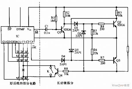
Simplified long-distance call lock is shown in the above picture. The lock can lock out the long-distance call without affecting the original function. It ispower-consuming, but it has very good compatibility. If switch K is placed as the picture shows, first dial the number “0”,, and you’ll find the “0” can not be dialed and the long-distance call can not be made while it does not affect dialing “0” when making local calls; if K is placed to the left, then the lock does not function. (View)
View full Circuit Diagram | Comments | Reading(1527)
Simplified Anti Toll Fraud Circuit Diagram
Published:2011/9/7 0:43:00 Author:Vicky | Keyword: Simplified Anti Toll Fraud Circuit
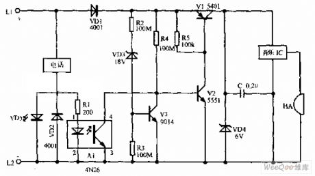
Simplified anti toll fraud circuit is shown in the above picture. The picture is a simplified anti toll fraud circuit. When the telephone is made normally, the indication light is luminous. When anyone wiretaps and makes calls, the circuit will give out fierce alarming sound which prevents the telephone from regular usage. The input lines of the circuit can be divided into positive and negative. The output lines can be connected with the telephone arbitrarily. (View)
View full Circuit Diagram | Comments | Reading(1109)
Bipolar Telephone Circuit Diagram
Published:2011/9/7 0:46:00 Author:Vicky | Keyword: Bipolar Telephone Circuit

Bipolar Telephone circuit is shown in the above picture. The circuit is a typical applied circuit of bipolar telephone IC SC34014. The circuit is simple, and the lowest work voltage is 1.5V when the call isunder usage. 34014 has a stabilized output voltage of 1.2V (providing working voltage for electret microphone); it has a stabilized DC voltage of 3.3V and current output of 550μ, and the current increases to 2mA when dialing. (View)
View full Circuit Diagram | Comments | Reading(2155)
Buick GL8 Car ABS Serial Data,SP205,Dynamical System ECU PCM And Other ECU Circuit
Published:2011/8/23 22:06:00 Author:Robert | Keyword: Buick, ABS, Serial Data, Dynamical System, ECU, PCM

The picture shows the Buick GL8 car ABS serial data, SP205, dynamical system ECU PCM, car body ECU BCM, combination instrument, ABS ECU, traction ECU EBCMEBTCB circuit. (View)
View full Circuit Diagram | Comments | Reading(1380)
RCC Power Practical Circuit Using Synchronous Rectification
Published:2011/8/23 22:06:00 Author:Robert | Keyword: RCC, Power, Practical, Synchronous, Rectification

The RCC power practical circuit by using synchronous rectification is shown in the picture. In the picture's dotted frame A, it is the control circuit which controls thereset currentto go through the saturable reactor ML. The output voltage is higher than the setting value, the reset current would increase. The larger of the reset current, the longer the time during ML to saturable would be. And also the wider the synchronous pulse width which is added to the secondary MOSFET (VF2) grid electrode would be. And the longer the conducted time of the secondary MOSFET would be. If the secondary MOSFET's conducted time is changed to be longer, even the transformer's flyback energy is fully released, the secondary MOSFET could also keep the conducted mode. The secondary smoothing capacity C1's voltage is added on the secondary winding and it would have the reverse excitation for the transformer. (View)
View full Circuit Diagram | Comments | Reading(932)
The regulator: DC-DC circuit and power supply monitor pin and its main features DS1705/DS1706
Published:2011/8/30 2:31:00 Author:Seven | Keyword: regulator, power supply, monitor pin

The DS1705/DS1706 monitorThe working voltage is 3.3V/5.0V; it has the halt and restart failure micro-processor; it can restart the micro-processor automatically after the computer fault is gone; it has the external overload monitor key; the 3.3V system can exactly monitor the resetting of 5%VCC, 10%VCC and 20%VCC; the 5.0V can monitor the resetting of 5%VCC or 10%VCC. The working temperature range is -40~85℃; the is compatible with MAX705/MAX706 completely. The definitions of its main pins are as follows: PBRST: input by pressing the reset key; IN: input; ST: triggering input.
(View)
View full Circuit Diagram | Comments | Reading(617)
The regulator: DC-DC circuit and power supply monitor pin and its main features DS1632
Published:2011/8/30 2:26:00 Author:Seven | Keyword: regulator, power supply, monitor pin

DS1632--the power supply fault and reset controllerThe working voltage is 5.0V; the computer power supply fault detector; there is a 32.768kHz oscillator on the chip; the clock is coupled with a cell; by pressing the reset key, the input can be done; the monitor precision is 5%VCC or 10%VCC; the reset pulse width is 95ms or 190ms; all the resetting, power supply fault and cell low-voltage are coupled with the additional output. The definitions of the pins are as follows: PBRST: input by pressing the reset key; X1 and X2: the crystal oscillator.
(View)
View full Circuit Diagram | Comments | Reading(528)
Three-Port CMOS Voltage Regulator Equivalent Circuit
Published:2011/8/23 22:07:00 Author:Robert | Keyword: Three-Port, CMOS, Voltage, Regulator, Equivalent

The three-port CMOS voltage regulator equivalent circuit is shown in the picture. Its internal control circuit is made up by the CMOS analog circuit. The output transistor uses the P-channel MOSFET (negatice output voltage uses N-channel MOSFET). The CMOS voltage regulator circuit's structure is simple. Many factories increase its performance by improving its manufacturing process. The CMOS voltage regulator's feature is that there are many products with low output voltage and low loading current, and they have low consumption current. They could be used as the power for charging the battery and local auxiliary power. (View)
View full Circuit Diagram | Comments | Reading(3992)
The regulator: DC-DC circuit, power supply monitor pin and its main features DS1231S
Published:2011/8/30 2:24:00 Author:Seven | Keyword: DC-DC circuit, power supply, monitor pin

The DS1231S power supply monitorThe working voltage is 5.0V; when the power supply fault is approaching, it will send the forecast to the processor; it provides the power failure lasting time; it can automatically restart the processor when the power is coming; the monitor precision is 5%Vcc or 10%Vcc; it can adjust the maintenance time of power saving; it can replace the power reset circuit. The main pins of it are as follows: IN: input; MODE: pin features selecting; TOL: choosing detection of 5%Vcc or 10%Vcc.
(View)
View full Circuit Diagram | Comments | Reading(505)
The regulator: DC-DC circuit, power supply monitor pin and its main features BA6122A/6122AF
Published:2011/8/24 21:51:00 Author:Seven | Keyword: DC-DC circuit, power supply, monitor pin

BA6122A/6122AF--The switch stabilizer control circuit (dual output) This is a switch stabilizer control circuit of dual output, which forms the 5V or 9V dual output switch stabilizer; it contains a 5V Vref circuit, sawtooth wave oscillating circuit, fault amplifier circuit, comparing circuit and output circuit; the working power supply voltage range is 8~16V; The 9V system has the stopping function; the drive load ratio changing range of the driver is 0~100%; the power consumption is 340mW; the working temperature is -10~+60℃. (View)
View full Circuit Diagram | Comments | Reading(660)
The regulator: DC-DC circuit, power supply monitor pin and its main features AN8360NK
Published:2011/8/24 21:50:00 Author:Seven | Keyword: DC-DC circuit, power supply, monitor pin

AN8360NK voltage charge control circuit This is a control circuit of the lead battery fast charging current; it can quickly charge the 4~12V lead battery (about 80min); the working voltage range is 8~19V; the charge reference signal is generated by 8-bit A/D converter; the max power supply voltage is 20V; the max power supply current is 33mA; the power consumption is 660mW; the working temperature is -20~75℃.
(View)
View full Circuit Diagram | Comments | Reading(696)
The regulator: DC-DC circuit, power supply monitor pin and its main features AN8060
Published:2011/8/24 21:50:00 Author:Seven | Keyword: DC-DC circuit, power supply, monitor pin

AN8060--the 4V stabilizer (with reset terminal) This is a stabilizer with the fixed output voltage; the output voltage is -4V; the max output current is 30mA; the minimum input-output voltage difference is lower than 0.2V; the input voltage range is -12~0.3V; the power consumption is 500mW; the working temperature is -20~+75℃; it contains the test comparator.
(View)
View full Circuit Diagram | Comments | Reading(803)
The regulator: DC-DC circuit, power supply monitor pin and its main features AN8050S
Published:2011/8/24 21:49:00 Author:Seven | Keyword: DC-DC circuit, power supply, monitor pin

AN8050S stabilizer (multiple input) This is a stabilizer of multiple input whose output voltage is fixed; the output voltage includes two teams of tracking voltages, which are ±5V and -4.3V; the output current of ±5V is +80mA, the output current of +5V is +50mA, and the output current of -4.3V is +10mA; the working power supply voltage range is ±2~±9V; the power consumption is 420mW; the working temperature is -20~+75℃; it contains the decompression test comparator and heat protection circuit.
(View)
View full Circuit Diagram | Comments | Reading(563)
| Pages:498/2234 At 20481482483484485486487488489490491492493494495496497498499500Under 20 |
Circuit Categories
power supply circuit
Amplifier Circuit
Basic Circuit
LED and Light Circuit
Sensor Circuit
Signal Processing
Electrical Equipment Circuit
Control Circuit
Remote Control Circuit
A/D-D/A Converter Circuit
Audio Circuit
Measuring and Test Circuit
Communication Circuit
Computer-Related Circuit
555 Circuit
Automotive Circuit
Repairing Circuit