
Circuit Diagram
Index 493
74 Series digital circuit of 74293,74LS293 4-bit binary counter
Published:2011/8/12 2:22:00 Author:Lucas | Keyword: 74 Series , digital circuit, 4-bit binary counter


Ithas zero gate input. Electrical performance and functionality are the same with the 7493A and 74LS93. It just changes the lead arrangement.
(View)
View full Circuit Diagram | Comments | Reading(3960)
MIC2298 LED driver circuit diagram
Published:2011/9/8 3:38:00 Author:Lucas | Keyword: LED driver
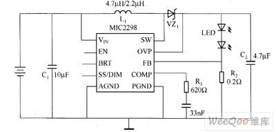
Micrellnc introduces the industry's smallest and most powerful LED driver MIC2298 for portable electronic devices. The device is the 7W efficient boost DC / DC converter, and it uses small 3mm × 3mm MLF packaging. MIC2298 is designed for mobile phones, personal digital assistant (PDA) and digital camera's flash and torch lighting applications. MIC2298 can ensure 3.5A conversion current. The operating input voltage range is 2.5 ~ 10V.
(View)
View full Circuit Diagram | Comments | Reading(1757)
MAX16831 White LED driver circuit diagram
Published:2011/8/23 22:22:00 Author:Lucas | Keyword: White LED driver
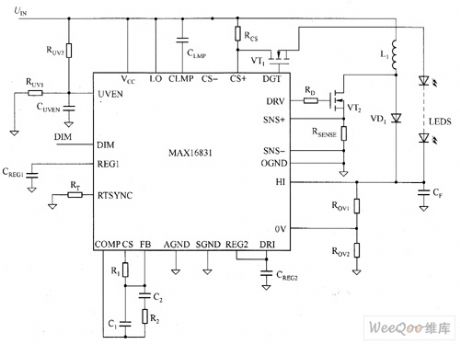
MAX16831's main technical characteristics are as follow. ① Wide Input Range: 6 ~ 76V, cold start working can be up 5.5V. ② integrated white LED current sense differential amplifier. ③ it can drive N-channel MOSFET with floating light drive capability. ④ white LED current accuracy: 5%. ⑤ 200Hz-chip ramp generator can be synchronized to an external PWM dimming signal. ⑥ its sync / programmable switching frequency is 125 ~ 600kHz. ⑦ iy has output over-voltage, open load, white LED short circuit, overheat protection. ⑧ enable / shutdown input, turn-off current is less than 45μA.
(View)
View full Circuit Diagram | Comments | Reading(854)
MAX6965 White LED driver circuit diagram
Published:2011/8/23 22:22:00 Author:Lucas | Keyword: White LED driver
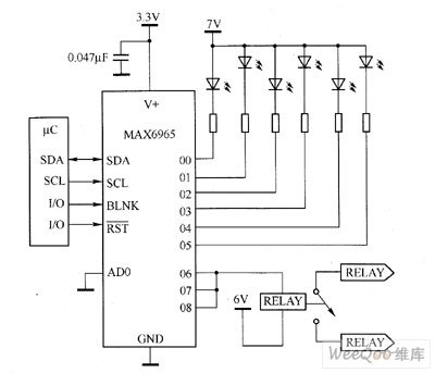
MAX6965's main technical characteristics are as follow. ① 400kbps, 2-wire Serial Interface, 5.5V voltage tolerance. ② 2 ~ 3.6V operating voltage. ③ 8-bit PWM White LED brightness control. ④ global 16 brightness control, additional 16 independent brightness control. ⑤ Rated Output 7V, open-drain. ⑥ two-phase flashing white LED. ⑦ high port output current, each port's output current is 50mA (max). ⑧ when it is in RST input clear port status, port status returns to power-on default state. ⑨ it supports hot insertion. ⑩ low standby current is typical 1.2μA, and the maximum value is 3.3μA.
(View)
View full Circuit Diagram | Comments | Reading(1101)
SR03x driving LED circuit diagram
Published:2011/8/23 22:22:00 Author:Lucas | Keyword: driving LED
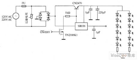
SR03x is the dual-output DC / DC power management IC without any magnetic components, the typical application circuit is shown as the figure. SR036 and SR037 are SR03x series of products produced by SUPERTEX company, and in the figure, SR03x series do not need any transformer, inductor, or high input capacitor. At the same time, its working principle is simple: SR03x input end is designed to access 120μV, 230V rectified output directly. SR03x series of IC requires only minimal external components.
(View)
View full Circuit Diagram | Comments | Reading(2156)
MAX7306/MAX7307 white LED driver circuit diagram
Published:2011/8/23 22:22:00 Author:Lucas | Keyword: white LED driver
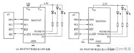
MAX7306/MAX7307's main technical characteristics are as follow. ① 1.4 ~ 5.5VI / O logic into port power (ULA). ② Power supply voltage is 1.62 ~ 3.6V. ③ It has independent 33 PWM brightness control with 15 flash control in output end, and 1kHz PWM cycle flicker-free white LED brightness control. ④ optional input debounce, input over-voltage is up to 5.5V (ULA) with interrupt output transient detection. ⑤ when it is in low-level active RST input clear port state, J will restore power-on default state. ⑥ oscillator input and output can cascade multiple devices. ⑦ low standby typical current is 0.75μA.
(View)
View full Circuit Diagram | Comments | Reading(772)
MAX7314 white LED driver circuit diagram
Published:2011/8/23 22:22:00 Author:Lucas | Keyword: white LED driver
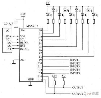
MAX7314's main technical characteristics are as follow. ① it has 400kbps, 2-wire serial interface, and the voltage is 5.5V. ② working voltage is 2 ~ 3.6V. ③ the total 8-bit PWM LED intensity control has a global 16-level brightness control with separate 16 additional brightness control, two-phase LED flashing. ④ it has Interrupt Output transition detection circuit, which can work in 5.5V open-drain output, each port's maximum output current is 50mA. ⑤ Input over-voltage protection is up to 5.5V. ⑥ operating current is typical 1.2μA, and the maximum value is 3.6μA. ⑦ it uses small 4mm × 4mm thin QFN package.
(View)
View full Circuit Diagram | Comments | Reading(780)
the circuit of the granary full reminder for the combine harvester (1)
Published:2011/8/11 4:39:00 Author:Ariel Wang | Keyword: granary full reminder, combine harvester

When the granary is not full,V1 is conducted by the infrared light emitted by VL.V2 is stopped.The pin-2 of IC becomes high level.The pin-3 outputs low level.It is released.HL isn’t lighted.HA doesn’t give a sound.When the granary is full,the food in granary covers YL and VI.The resistence of VL is large.1 and 2 are conducted.The high level of IC’s pin-2 becomes low level. The monostable circuit turns over.The pin-3 of IC outputs high level.K is conducted to pull in.The normally open contacts are conducted.HL is lighted.HA gives out alarm sound.It tells the driver that the granary is full. (View)
View full Circuit Diagram | Comments | Reading(529)
the expansion circuit of a 8-bits parallel port of PI port
Published:2011/8/11 4:01:00 Author:Ariel Wang | Keyword: expansion, 8-bits , parallel, port, PI

If there are toomany expansions and strobe signals take too many bits of parallel ports.For example,if you want to expand 8 parallel output ports.Then you need 8 signals.At this time,just these signals can take 8-bits parallel ports.Such huge resources wasting phenomena in singlechip system with limited I/O port linesare not tolerable.It adopts chip 74HC573( octal transparent type D flip-latch with three state output) to expand p1 port with 8-bits parallel port.Strobe signal adopts P3.3's pin of P3 port. The principle diagram is as seen as above.
(View)
View full Circuit Diagram | Comments | Reading(684)
the diode and triode online testing machine composed of 556
Published:2011/9/8 6:15:00 Author:Ariel Wang | Keyword: diode, triode , online testing machine

The monostable trigger is composed of the other half of 556.The pin ⑤ and pin ⑨ of 556 output 5Hz alternating square wave of which the peak voltage with a pair of reversed polarities is 9V . When the power supply gets through,if LED1 and LED2 give out light alternately without devices (the tubes),then the testing signal souce is normal.If you want to indicate whether the diode and triode are OK or not,distinguish the polarity of the tubes,testing conditions,whether LED1 and LED2 are lighted or not and the testing results quickly with the tubes(i.e. There are lines),you can refer to the chart. (View)
View full Circuit Diagram | Comments | Reading(587)
the quick SCR testing machine composed of 555
Published:2011/9/8 6:15:00 Author:Ariel Wang | Keyword: SCR, testing machine

The oscillation frequency shown in the chart is about 1Hz.The charging time t of the capacitor C =0.693(R1+R2)C.The discharge time t of the capocitor C =0.693R2C.They are quite alike.So the duty cycle of the output pulses is near 1:1. LED1,resistor R4,SCR,transistor BG2 form a closed circuit when 555 outputs high level as AN is pressed and SCR is plugged in.LED1 gives out light.LED2,R4,SCR and BG1 form a closed circuit when 555 outputs low level.LED2 gives out light.It indicates the SCR is good. (View)
View full Circuit Diagram | Comments | Reading(1323)
the digital capacitor testing machine
Published:2011/9/8 6:15:00 Author:Ariel Wang | Keyword: digital capacitor, testing machine

the counting circuit IC3 adopts double BCD addition counter CD4518.IC4 and IC adopt BCD-seven-segment-latch,decoding driver CD4518.LED adopts common cathode LED which matches CD4511.You can adjust the potentiometer W1,W2 to correct the testing machine.In this way,you can get the frequency signals of 9.09kHz and 0.909kHz.You can put the selectorswitch K2 to position 1 .Then the potentiometer W1 is shortcut with resistance R6.You can adjust the potentiometer W2.In this way the output cycle becomes 1.1ms(9.09kHz).Then you can put the selectorswitch K2 to position 2 .You can adjust the potentiometer W1.In this way the output cycle becomes 11ms(0.909kHz).
(View)
View full Circuit Diagram | Comments | Reading(1383)
the multifunction electronic probe and instrument composed of 555
Published:2011/9/8 6:16:00 Author:Ariel Wang | Keyword: multifunction, electronic probe , instrument

You can plug two electrodes in CK1.The oscillation frequency becomes higher as the resistance of the points is low.When the distance between the points and the detectors becomes farther,the frequency becomes lower.In this way it is to reach the points detection.The timer is made up by ICl(555),R5,W2 and C3.The pulse generator is the multivibrator composed of W4,R8,D3,D4,W3 and C4.The oscillation frequency is f=1.44/(Rw4+R8+Rw3)C4.You can adjust the potentiometer W3 and W4 to change the oscillation frequency and duty ratio.
(View)
View full Circuit Diagram | Comments | Reading(581)
The remote controller of drainage and irrigation pumping station
Published:2011/9/6 4:43:00 Author:Felicity | Keyword: remote controller, drainage and irrigation pumping station

On remote start, press S3, and the phase voltage of L3 goes through the normally open contact of S3 to put on KM, And KM turns on, and the normally open contact KM1, KM2 closes and the pump motor starts. After release S3, the phase voltage of L3 goes through FU2, HL, S2, normally open contact KM2, KM and the normally close contact of KR to phase L2 to make up circuit and maintaining KM close.When it needs to stop, press S4 to make KM off and the pump motor M stops.
(View)
View full Circuit Diagram | Comments | Reading(807)
Colourful Lights Controller Twenty-nine
Published:2011/8/12 4:50:00 Author:Felicity | Keyword: Colourful Lights Controller

This colourful lights controller contains SH804 or SH805 colourful lights oriented controller IC.SH-804,SH-805 are the same with SH803 in shape,inner circuit and application circuit, while the stored control program and the function of pins are different. SH-804 has 10 lights repetition modes and 6 change speeds.The modes can cycle automatically or be set by control buttons. SH-805 has 16 repetition modes which can be set by control buttons. The application circuits of SH-804 and SH-805 are shown in Fig.1-144 and Fig.1-145,the select of components of which can refer to the application part of SH-803. (View)
View full Circuit Diagram | Comments | Reading(864)
Timing Controller (the 2nd)
Published:2011/8/12 4:53:00 Author:Felicity | Keyword: Timing Controller

Work of the circuit
The circuit consists of Power supply circuit, pulse generator, control implementation delay circuit and control circuit. ( It is showed in picture 8-91.)
Power supply circuit consists of buck capacitor Cl, discharge resistor R7, voltage regulator diode VS, the rectifier diode VDl and filter capacitor C2.
Pulse generator consists of time-base integrated circuit ICl, resistors Rl and R2, potentiometers RP and capacitors C3.
Control implementation delay circuit consists of decimal counting / pulse distributor circuit IC2, resistors R3 and R4, diode VD2-VD11, switch S1-S12.
Control circuit consists of transistor V, resistors R5 and R6, thyristor VT and AC contactor KM. (View)
View full Circuit Diagram | Comments | Reading(918)
Liquid Level Controller (the 2nd)
Published:2011/8/12 4:52:00 Author:Felicity | Keyword: Liquid Level Controller

Work of the circuit
The circuit consists of power circuit and level detection and control circuit. (It is showed in picture 8-100.)
The power circuit consists of power transformer T, bridge rectifier UR and filter capacitor Cl, C2.
Level detection and control circuit consists of level electrode AC, four NAND gate IC IC (Dl-D4), the transistor V, resistors Rl-R3, relay K and diode VD.
220V AC voltage is bucked by T ,rectified by UR and filtered by C1, C2. It then supplies 12V voltage to relay K and IC. (View)
View full Circuit Diagram | Comments | Reading(1253)
The circuit diagram of the high gain band-pass filter (LM307) with low Q
Published:2011/8/12 4:54:00 Author:Felicity | Keyword: high gain, band-pass filter


The circuit of the high gain band-pass filter with low Q is shown in this figure. Adding multiple feedback circuit to operational amplifier can build up a high gain band-pass active filter with low Q. This circuit adopts LM307 operational amplifier, using the components’ parameters in this figure to calculate: BW is the bandwidth when the gain of the operational amplifier is 1.
(View)
View full Circuit Diagram | Comments | Reading(1247)
the absolutely useful switch power supply :the C7428 power supply(A4)
Published:2011/8/20 2:20:00 Author: | Keyword: absolutely useful, switch power supply

View full Circuit Diagram | Comments | Reading(839)
The Typical Circuit Diagram of Monolithick Color Scanner (LM9832)
Published:2011/9/8 6:19:00 Author:Ariel Wang | Keyword: Typical , Monolithick, scanner


The circuit is constituted by the LM9832 typical single color scanner . RSENSE is the stepper motor current sense resistor. VT1 ~ VT4 are external drive tubes. LM9832 uses a USB interface.The data receives and sends through the D + and D-pins. These data is 3V differential signal. The circuit between LM9832 D + , D-pins-chip and the color scanner with a USB connector could be seen as the chart. R1 and R2 are two data lines limiting resistor. C1 and C2 are the capacitors to eliminate noise.R3 is the pull-up resistor , R4 is the pull-down resistor.
(View)
View full Circuit Diagram | Comments | Reading(1300)
| Pages:493/2234 At 20481482483484485486487488489490491492493494495496497498499500Under 20 |
Circuit Categories
power supply circuit
Amplifier Circuit
Basic Circuit
LED and Light Circuit
Sensor Circuit
Signal Processing
Electrical Equipment Circuit
Control Circuit
Remote Control Circuit
A/D-D/A Converter Circuit
Audio Circuit
Measuring and Test Circuit
Communication Circuit
Computer-Related Circuit
555 Circuit
Automotive Circuit
Repairing Circuit