
Circuit Diagram
Index 492
Double contact-plate resistance bridge touch switch circuit diagram
Published:2011/9/9 8:00:00 Author:Vicky | Keyword: double contact-plate, resistance bridge touch switch


Resistance bridge touch switch in the picture 1 is composed of LM339. LM339 is a a quad voltage comparator (with 4 identical voltage comparator inside). The circuit only takes use of one of the four. Work voltage range reaches 2-32V. When hands are very close to the double metal plate but not touch them, pin2 of LM339 outputs low level signal, which makes the luminous diode LED1 conducted and lightened.
The difference of the resistance bridge touch switch in the picture 2 from picture 1 lies in that it adopts calculating amplifier LF353N instead of voltage comparator. (View)
View full Circuit Diagram | Comments | Reading(2081)
Wireless telephone adaptor circuit diagram
Published:2011/9/9 7:42:00 Author:Vicky | Keyword: wireless, telephone adaptor
Wireless telephone adaptor circuit is shown in the above picture. The composition of the wireless telephone adaptor is very simple and the cost is very low, while the function is complete and practical. Its functions are listed below: after adding the adaptor, the average wireless can dial two external lines of different region arbitrarily in accordance with one’s demands, which equals two wireless telephone actually. As the user with many extensions, it can also realize making calls among the extensions, and the function of tallback. (View)
View full Circuit Diagram | Comments | Reading(1911)
Schematic and applied circuit diagram of pulse circuit composed of photoelectric coupler
Published:2011/9/9 7:54:00 Author:Vicky | Keyword: Schematic and applied circuit diagram, pulse circuit composed of photoelectric coupler

picture1
picture2
When Ec is just on in picture 1(a), Up increases when C is charging. When UF≈1, luminous diode and then the triode become saturate, and output Uo≈Ec.
When triode becomes saturate, C discharges (through two route: C→F→E1→Er and C→RF→+Ec→R ). Uo becomes lower. The diode stops when c discharges to a certain degree. The triode stops subsequently after moving all the memory electric charge, and uo becomes zero. Power Ec charges C again after triode stops, and the above process repeats again. Thus the peak output wave is obtained, and the cycle is (when RF》Re ): T=C(RF+Re)In2 (View)
View full Circuit Diagram | Comments | Reading(992)
Complementary tube pulse circuit principle and applied circuit diagram
Published:2011/9/9 7:51:00 Author:Vicky | Keyword: complementary tube pulse circuit

(picture1)
Complementary tube bistable state circuit is shown in picture1(a). When the power is on, if no triggering signal works, the two tubes stop working and the state is in a stable state because the collector current is extramely small, and the end voltage of RC1, and Rc2 (bias current provided to the two tubes) is also very small.
When the trigger pulse is working, suppose that BG1 becomes amplified from static, and leads to the process of avalanche-type positive feedback. Soon the two tubes become saturate, and are in another stable state. Capacitance C1 is speed-up capacitor. From picture1(b), we can see that uc1 goes down to zero sharply from Ec, while Uc2 zooms up to Ec from zero. (View)
View full Circuit Diagram | Comments | Reading(998)
Schematic and applied circuit diagram of tunnel diode pulse circuit
Published:2011/9/9 7:56:00 Author:Vicky | Keyword: tunnel diode pulse circuit

Volt-ampere characteristics and parameter of tunnel diode
Volt-ampere characteristics of tunnel diode (see picture a) is a S pattern curve. The highest current point P in the curve is called the peak; the lowest current point V is called valley point. The main parameters of the tunnel diode are:
(1) Peak point voltage Up is about dozens of millivolt; valley point voltage Uv is about hundreds of millivolt.
(2) Peak point current Ipi is about several milliampere; valley point voltage Iv is about hundreds of microampere.
(3) Proportion of peak point current and valley point current is about 5-6; the higher, the better.
(4) Valley point capacitance Cv of from several microfarad to dozens of microfarad, and the lower, the better; 2BS4A made in China: Up=80 millivolt, Ip = 4 milliampere, valley point current proportion ≥5, Cv = 10~15 microfarad, Uv = 280 millivolt. (View)
View full Circuit Diagram | Comments | Reading(1328)
Circuit diagram of small-size battery charger available to choosing charging time
Published:2011/9/9 8:01:00 Author:Vicky | Keyword: small-size battery charger , choosing charging time

Small-size battery charging circuit which can choose charging time is shown in the above picture. The charger has the required constant current source digital circuit timer for charging safely. It can be used to charge 12 pieces of nickel-cadmium batteries. There are three grades of charging time for choice, and they are 5 hours, 14 hours, and 24 hours. The voltage adaptor of 15V outputs voltage supply the power for the circuit. 15V DC voltage is sent to the two constant current sources to charge the battery. In addition, IC3 (7810) provides the stable 10V power voltage for the timer。 (View)
View full Circuit Diagram | Comments | Reading(1583)
Frequency Synthesizer Circuit Composed of MSM5820RS
Published:2011/8/25 7:42:00 Author:Sue | Keyword: Frequency Synthesizer

The picture shows the frequency Synthesizer circuit which is composed of MSM5820RS. The circuit uses 400HZ as center and it realises ±10% frequencyregulation by adjusting FP1's resistance value. S1 is reset switch. The oscillating circuit of 2MHz which is composed of TC5082P and crystal will output frequency signal of 500KHZ through pin 5 after it is frequency divided by TC40H074P. The signal will be put on MSM5820RS's pin 27 and then it will output signal from pin 6.
(View)
View full Circuit Diagram | Comments | Reading(4351)
Oscillating Circuit Composed of SN7490
Published:2011/8/25 7:42:00 Author:Sue | Keyword: Oscillating Circuit

The picture shows the oscillating circuit which is composed of SN7490. In the circuit, the oscillating circuit uses TTL GATE circuit with a oscillate frequency of 1MHZ. When the six frequency dividing circuits SN7490 are connected in parallel, they can divide frequency and generate a frequency signal of 1HZ. The circuit's A,B,C,D,E,F terminals will output signals of frequency of 100kHZ, 10kHZ, 1kHZ, 100HZ, 10HZ and 1HZ. (View)
View full Circuit Diagram | Comments | Reading(3460)
Oscillating Circuit Composed of TC5082P
Published:2011/8/25 7:45:00 Author:Sue | Keyword: Oscillating Circuit

The picture shows the oscillating circuit which is composed of TC5082P. TC5082Pis a kind of integrated circuit which is used by PLL frequency synthesizer with 12 grade frequency divided circuit inside, and it has a wide use range. If the crystal oscillator's frequency is 10.24KHZ, then TC5028P's pin 8 can outputa signal of frequency of 40kHZ and its pin 7 can output a signal of frequency of 10kHZ, pin 6 can output a signal of frequency of 5kHZ, pin 4 can output a signal of frequency of 2.5 kHZ. If TC4017 and TC4024 are connected, then TC5028P's pin 8 will output a signal of frequency of 40kHZ, which will output a signal of frequency of 4KHZ on B terminal after it is frequency divided by TC4017P10.
(View)
View full Circuit Diagram | Comments | Reading(1754)
Reversible Running Illumination Controller(C043,C301,C188,C003)
Published:2011/8/25 7:43:00 Author:Sue | Keyword: Reversible, Running Illumination, Controller

When IC2'spin 9 outputs high level, this level signal will be put on IC3's CP terminal and will make it reverse. IC1's U/D terminal will become high level.Then IC1 will begin to count by subtraction from next clock pulse which will make the controlled illumination be turned on by turns from 9 - 0 . When IC2's 0 terminal outputs high level, the above-mentioned process will be repeated which will make IC1 begin to count by addition. So the repetition of the above-mentioned process can realise the reversible control of the running illuminations.
Besides, by adjusting potentiometer w in the circuit, the running speed can be adjusted.What's more, ifresistance value of resistor R2 is increased properly, the running speed of the illuminations can be lower than 0.5HZ. (View)
View full Circuit Diagram | Comments | Reading(626)
Rolling Circle Motive Display Circuit Composed of CD4017
Published:2011/8/25 7:44:00 Author:Sue | Keyword: Rolling Circle, Motive, Display

As seen in the figure, because of CD4017's output trait thatone of its10 output terminals will output high level while the other nine terminals all output low level, CD4017 is connected to be sink current output condition to constitute a rolling circle display circuit. (View)
View full Circuit Diagram | Comments | Reading(2477)
Advertising Decor Lamp Controller Composed of 555
Published:2011/8/25 7:47:00 Author:Sue | Keyword: Advertising Decor Lamp, Controller

IC1 and R1,R2,C1 constitute multivibrator and its oscillating frequency f=1.44/(R1+2R2). The corresponding parameter in the circuit is about 4Hz. As seen in the figure (b), we can see from B that IC2 and R3,R4,C2 constitute trigger circuit which will realise two frequency division of IC1's output square wave A. As seen in the figure (b), we can see from C that IC3 and R5,R6,C3 constitute trigger circuit which will realise three frequency division of IC1's output square wave A. As seen in the figure (b), we can see from D that IC4 and R7,R8,C4 constitute trigger circuit which will realise six frequency division of IC1's output square wave A. (View)
View full Circuit Diagram | Comments | Reading(629)
Sine Wave Oscillating Circuit Compsoed of MJM5534
Published:2011/8/25 7:46:00 Author:Sue | Keyword: Sine Wave, Oscillating Circuit

The picture shows sine wave oscillating circuit which is composed of MJM5534. This a kind of wien bridge sine wave oscillating circuit. If R1=R2=R,C1=C2=C, then oscillating frequency is 1/(2πRC). Wien bridge will make amplitude stay stable, so there is great distortion. But when it is converted to low frequency which is below 10HZ, the amplitude will be stable in short time. According to the component parameter in the picture, by adjusting RP1's resistance value, output voltage's effective value is 5V. By changing C1's value, its distortion rate will be 0.7%-0.9% in the frequency range of 10HZ-100KHZ. If output voltage's effective value is adjusted to 3V, then the distortion rate can be reduced to 0.1%. (View)
View full Circuit Diagram | Comments | Reading(697)
Voltage/Frequency Converter Counting Display Circuit Composed of 555
Published:2011/8/25 7:45:00 Author:Sue | Keyword: Voltage/Frequency Converter, Counting Display

The picture shows the voltage/frequency converter counting display circuit composed of 555. (View)
View full Circuit Diagram | Comments | Reading(562)
CAT3606 white LED driver circuit diagram
Published:2011/8/23 22:23:00 Author:Lucas | Keyword: white LED driver
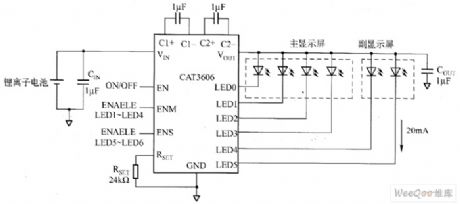
CAT3606 and lithium-ion battery system are used in conjunction to get 90% efficiency, the current of each output channel can be adjusted to match up to 6 white LEDs and make consistency brightness of control panel. Its unique fractional charge pump technology can automatically switch 1x mode to 1.5x mode to ensure that the entire life of the battery remains flicker-free white LED current. CAT3606 uses 16-pin 4mm × 4mm QFN package with a maximum height of 0.8mm, the product uses green packaging materials without halogen and lead, and it can reach R0HS requirements.
(View)
View full Circuit Diagram | Comments | Reading(836)
MAX7316 white LED driver circuit diagram
Published:2011/8/23 22:23:00 Author:Lucas | Keyword: white LED driver
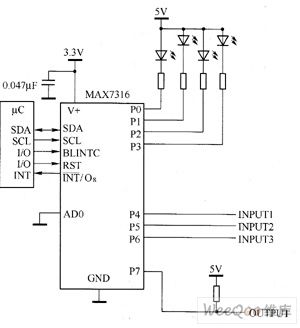
MAX7316's main technical characteristics are as follow. ① 400kbps, 2-wire Serial Interface, 5.5V voltage tolerance. ② working voltage is 2 ~ 3.6V. ③ 8-bit PWM White LED brightness control, global brightness control 16 with additional 16 independent brightness control. ④ two-phase flashing white LED. ⑤ it has 5.5V input voltage protection. RST input clears the serial port status, and restore it to power-on default state. ⑥ each high port output current is 50mA (max); output voltage is 5.5V, open-drain. ⑦ it supports hot insertion. ⑧ low standby current is typically 1.2μA, and the maximum value is 3.3μA.
(View)
View full Circuit Diagram | Comments | Reading(1399)
MAX16809/MAX16810 white LED driver circuit diagram
Published:2011/8/23 22:23:00 Author:Lucas | Keyword: white LED driver
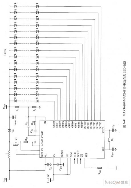
MAX16809/MAX16810's main technical characteristics are as follow. ① it has 16 constant current output channels (each channel is up to 55mA), each output has ± 3% current matching. ② all channels uses a single resistor to set the white LED current. ③ parallel output channels can provide greater white LED series branch current. ④ continuous rated output voltage is 36V. ⑤ output enable pin is used for PWM dimming (frequency is up to 30kHz). ⑥ it has white LED open detection circuit and watchdog (MAX16810). ⑦ it has wide dimming ratio, which can be up to 5000:1.
(View)
View full Circuit Diagram | Comments | Reading(967)
MAX16807/MAX16808 white LED driver circuit diagram
Published:2011/8/23 22:22:00 Author:Lucas | Keyword: white LED driver
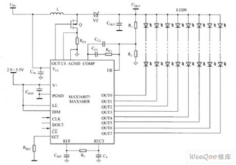
MAX16807/MAX16808's main technical characteristics are as follow. ① it has 8 constant current output channels (each channel current is up to 55mA). ② the current matching accuracy of output end is ± 3%. ③ parallel channels make each branch have a greater series white LED current. ④ continuous rated output voltage is 36V. ⑤ output enable pin is used for PWM brightness adjustment (frequency is up to 30kHz). ⑥ it can use a single resistor to set the white LED current for all channels. ⑦ wide brightness ratio is up to 5000:1. ⑧ low current detection reference (300mV) could achieve high efficiency.
(View)
View full Circuit Diagram | Comments | Reading(1038)
MAX8901A/MAX8901B white LED driver circuit diagram
Published:2011/8/23 22:22:00 Author:Lucas | Keyword: white LED driver
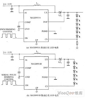
MAX8901A/MAX8901B boost converter is capable of driving 2 to 6 series white LEDs with constant current, and it can provide white LED drivers with uniform brightness and LCD backlighting for mobile phone, PDA and other handheld devices. MIAX8901A/MAX8901B's main technical characteristics are as follow. ① efficiency is up to 91%. ②it has 2.6 ~ 5.5V input voltage range. ③ it has fixed frequency mode. ④it has input undervoltage lockout, input overvoltage lockout, white LED overvoltage protection function (typical value is 25V). ⑤ typical shutdown current is 0.01μA. It has no white LED current under shutdown mode.
(View)
View full Circuit Diagram | Comments | Reading(1398)
74 series digital circuit of 74LS398/399 4-bit 2-to-1 data selector
Published:2011/8/11 3:20:00 Author:Lucas | Keyword: 74 series , digital circuit, 4-bit , 2-to-1 data selector


a1, a2 ...= A1, A2 ... steady input level. QA0, QB0 ...= QA, QB ... level before the establishment of steady-state input conditions.74LS398/ 74LS399, 74F398/ 74LS399, 74S398/ 74LS399 4-bit 2-to-1 data selector 74LS398 has dual-ended output, and 74LS399 has single-ended output; 74LS398 and 74LS298 are similar, and they use the reverse phase clock.
(View)
View full Circuit Diagram | Comments | Reading(1000)
| Pages:492/2234 At 20481482483484485486487488489490491492493494495496497498499500Under 20 |
Circuit Categories
power supply circuit
Amplifier Circuit
Basic Circuit
LED and Light Circuit
Sensor Circuit
Signal Processing
Electrical Equipment Circuit
Control Circuit
Remote Control Circuit
A/D-D/A Converter Circuit
Audio Circuit
Measuring and Test Circuit
Communication Circuit
Computer-Related Circuit
555 Circuit
Automotive Circuit
Repairing Circuit