
Circuit Diagram
Index 490
the frequency calibrator composed of CD4046
Published:2011/9/9 19:44:00 Author:Ariel Wang | Keyword: frequency calibrator

You can make up a frequency calibrator by using the frequency locking characteristics of the phase-locked loop circuit.Other circuit composition is seen as the chart.The circuit consists of input signal amplification and shaping circuit, the standard frequency signal circuit, the signal comparative detection circuit and detection result indication circuit.
(View)
View full Circuit Diagram | Comments | Reading(1424)
12 bit D/A Commutator with Parallel Ports
Published:2011/9/4 7:32:00 Author:Joyce | Keyword: 12 bit, D/A , Commutator , Parallel Ports

DAC1210 is compatible with end I/O of the bus line of PCXT. Its reference voltage is provided by external circuit with 12 bit data parallel transmission. It has the structure of pair register. Due to parallel connection, the data conversion speed is fast (≤1μs) .Similar models are DAC1208, DAC1209, MP1209, MP1210, which are commonly used in industrial automation control and automatic measurement circuits. As shown in the figure is its typical application circuit. (View)
View full Circuit Diagram | Comments | Reading(1009)
The responsiveness tester composed of CD4017
Published:2011/9/9 19:50:00 Author:Ariel Wang | Keyword: responsiveness tester

The responsiveness tester used to test response capabilities and training of human rapid-response capability.It has a variety of structural forms.As shown in the chart the responsiveness tester uses the decimal counterCD4017 and light-emitting diodes.The structure is relatively simple, it can be used as a toy to train and test the children's rapid response capability. (View)
View full Circuit Diagram | Comments | Reading(741)
Nokia 7xxx Mobile Schematic Diagram 07
Published:2011/9/4 7:31:00 Author:Joyce | Keyword: Mobile, Schematic
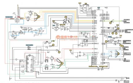
View full Circuit Diagram | Comments | Reading(3326)
Economical Fluorescence Display Circuit Composed of 555
Published:2011/9/4 7:31:00 Author:Joyce | Keyword: Economical, Fluorescence , Display

As shown in the figure is an economical fluorescence display circuit. The core of the circuit is a multivibrator composed of 555 ,R1, R2,and C1 ect, whose oscillation frequency is: f = 1.44 / (R1 + 2 R2)C1, the frequency of the corresponding parameters in the figure above being about 4 kHz. DC bias of the filament in the figure is : VDD ·R4/ (R3 + R4) ≈ 6 V. Adding a dc voltage of 6 V and an nkHz ac voltage whose Vp-p voltage is about 4 V to the filament of the fluorescent character-display tube on the calculator would make the fluorescent character display tube display. The structure of the circuit is simple thus it is easy to make. (View)
View full Circuit Diagram | Comments | Reading(1021)
Scanning Oscillating Circuit Composed of TL082
Published:2011/9/4 7:30:00 Author:Joyce | Keyword: Scanning, Oscillating

This is a scanning oscillating circuit composed of TL082, which can get voltage proportional to the control voltage Uc. If adding an antilog circuit when scanning logarithms, it can be used as an automatical scanner of sawtooth wave input and voltage-controlled oscillator of low frequency sine output. The circuit is composed of Wien bridge oscillating circuit and variable resistances (photo resistances within optical couplers PC1 ~ PC3) etc. Wien bridge circuit has a resistance capacitance network with frequency selectivity. The gain of A1 is about 3,and that of the loop is 1.Its oscillation frequency f is: f = 1 / (2πR0C0), in which C0 = C1 = C2, R0 = R1 + RG1 = R2 + RG2.
(View)
View full Circuit Diagram | Comments | Reading(1653)
Direction Displayer of Tape Movement
Published:2011/9/4 7:30:00 Author:Joyce | Keyword: Direction, Displayer, Tape, Movement

As shown in the figure is a direction display circuit of tape movement. The circuit is composed of rectangular pulse generator, D flip-flop (T077), decode circuit, light emitting diodes LED1 ~ LED4 etc. The rectangular pulse generator is composed of NAND gates YF1 ~ YF4, and its output signal frequency is 1 ~ 3 Hz, which can be changed by adjusting the value of C1, R1. T077 is connected in a state of counting, which will dichotomise the signal output by the rectangular pulse generator. The decode circuit constitutes of NAND gates YF5 ~ YF8, and its output signal will control the display of the led. (View)
View full Circuit Diagram | Comments | Reading(520)
Radio Digital Ondoscope
Published:2011/9/4 7:29:00 Author:Joyce | Keyword: Radio Digital Ondoscope

As shown in the circuit is a radio digital ondoscope circuit. It is composed of double time-base circuit 556( IC1), BCD code three bit counter IC2 (MC4553), 12 bit binary serial counter/frequency divider IC4 ( C040), BCD code seven segment lock /decode/driver and 4 digital luminescence tubes etc.
(View)
View full Circuit Diagram | Comments | Reading(1378)
Output of Triangle Wave and Square Wave Voltage-controlled Oscillation Circuit Composed of LF356
Published:2011/9/4 7:28:00 Author:Joyce | Keyword: Output , Triangle Wave, Square Wave , Voltage-controlled , Oscillation

This is the voltage-controlled oscillation circuit of triangle wave and square wave output composed of LF356. Voltage controlled oscillation circuit can be used as PLL circuit and scanning oscillation circuit. The circuit constitutes of polarity commutation circuit VT1, inverse integrator A2 and lag comparator A3 etc. VT1 constitutes a polarity commutation circuit, which works by switch. A1 can work in phase and inverse alternatively. When VT1 breaks over, A1 forms an inverting amplifier; when it cuts off, A1 forms an inphase amplifier. Integral circuit A2 can integrate voltage 士Uc which have been polarity commutated.
(View)
View full Circuit Diagram | Comments | Reading(1386)
Temperature system analog circuit for Resistance temperature detector
Published:2011/9/9 2:59:00 Author:John | Keyword: Temperature system analog circuit, Resistance temperature detector

The resistance of resistance temperature detector changes as the temperature changes. Commonly used materials for resistance temperature detectors are nickel, copper and platinum. And the platinum resistance temperature detector of 100 Ω~1000 Ω is the most common type. Resistance temperature detectors are suitable for linear response of temperature measurement within -200 ° C to +800 ° C. A resistance temperature detector includes three or four wires. Figure 2 shows the connection diagram for 3-wire resistance temperature detector and the analog converter. And RL1, RL2 and RL3 respectively represent the wire’s resistance for resistance temperature detector. (View)
View full Circuit Diagram | Comments | Reading(1344)
Bell generator circuit
Published:2011/9/9 2:28:00 Author:John | Keyword: Bell generator

Bell generator’s deep and lingering bell can lead people into a profound mood. As shown in the circuit, AN is clicked to voice “dang” and the sound is prolonged until slowly weakening. R1 and C1 in the figure determine the tone of the oscillator. R1 can choose between the 50K ~ 500K and C1 can choose between 103 and 503.
(View)
View full Circuit Diagram | Comments | Reading(762)
Tremolo amplifier circuit
Published:2011/9/9 2:24:00 Author:John | Keyword: Tremolo amplifier

The amplifier utilizes undersonic frequency (usually 5 ~ 15Hz) to do amplitude modulation for the audio input signal. The used National's LM389 IC contains three transistors and a power amplifier in the internal array. These transistors constitute the differential pair and active current source tail end. The differential amplifier output is proportional with two input signals’ product. Gain control potentiometer is used to adjust the desired tremolo intensity. R, C network within levels constitute the 160Hz high-pass filter and the tremolo frequency is required below 160Hz.
(View)
View full Circuit Diagram | Comments | Reading(1777)
Voice recording control circuit
Published:2011/9/9 2:09:00 Author:John | Keyword: Voice recording control
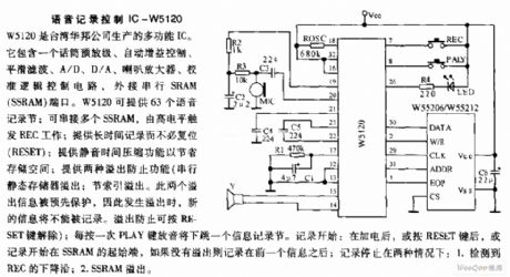
W5120 is a multifunctional IC produced by Taiwan's Winbond Company. It contains a microphone top-level, automatic gain control, smoothing filter, A / D, D / A, speaker amplifier, calibration logic control point and external Serial SRAM (SSRAM) port. W5120 provides 63 voice recording sections. It can cascade multiple SSRAM, whose high level triggers the REC to work. And it provides long records without needs to reset (RESET). Quiet time compression is provided to save storage space. Besides, two overflow prevention functions are equipped (Serial SRAM is easy to overflow and so is the section index.)
(View)
View full Circuit Diagram | Comments | Reading(1610)
Level Instruction Drive Circuit
Published:2011/9/4 7:26:00 Author:Joyce | Keyword: Level , Instruction , Drive
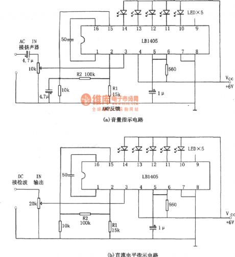
As shown in the figure is the LB1405 / LB1415 level instruction drive circuit. Figure (a) is an application circuit of LB1405 / LB1415 used as volume instruction, and figure (b) is an application circuit of LB1405 / LB1415 used as dc level instruction. The corresponding closed-loop gain of figure (a) is R2 / R1.Adjusting the 10 kΩ potentiometer will get the point of 0 dB. In the circuit, five stick leds are used to indicate the level of input signal. (View)
View full Circuit Diagram | Comments | Reading(3149)
Language filter circuit
Published:2011/9/9 1:56:00 Author:John | Keyword: Language filter circuit

The circuit can be used to limit the language frequency band, which can remove interference and noise except the clatter. This function can be achieved by two multiple negative feedback with two second-order active filters. Two filters are set in a cascaded manner, whose pre-end is the high-pass filter and pro-end is the low-pass filter. The overall characteristics appear to be that of the band-pass filter. High-pass filter’s cutoff frequency is 300Hz, which can constitute the lower end of band-pass filter; and low-pass filter’s cutoff frequency is 3000Hz, which can constitute a higher end of band-pass filter. The rolling band’s attenuation is 40 dB per 10 octave and the circuit’s gain is 1.
(View)
View full Circuit Diagram | Comments | Reading(723)
Detailed introduction to lims Laboratory Information Management System
Published:2011/9/9 1:44:00 Author:John | Keyword: Laboratory Information Management System
(1) Architecture for enterprise or laboratory network (enterprise can achieve by itself) In order to achieve the LIMS system, enterprise or laboratory network system should be built firstly (in-state local area network). And plan and layout should be made properly.
(2) Architecture for systemic management rightsThe module of systemic management rights (Ai real body) is used to complete various types of additions, deletions and authorization management for all landing system users. It can also authenticate the logging users. Different modules’ (Ai real body) functions are used according to their authority. (View)
View full Circuit Diagram | Comments | Reading(738)
The regulator: DC-DC circuit and power supply monitor pin and its main features DS1832
Published:2011/9/10 18:59:00 Author:Seven | Keyword: regulator, power supply, monitor pin

The DS1832 voltage monitorThe working voltage is 3.3V; the halt and restart failure micro-computer; the microprocessor restarts automatically after the power supply fault is gone; it is used in external overload monitor keys; the monitor precision is 10%Vcc or 20%Vcc; the working temperature is -40~85℃; it can replace DS1232. The definitions of the main pins are as follows:PBRST : input by pressing the reset key; TD: the time delay setting; TOL: selecting the 10%Vcc or 20%Vcc monitor; PBRST: triggering input.
(View)
View full Circuit Diagram | Comments | Reading(610)
The regulator: DC-DC circuit, power supply monitor pin and its main features LM199AH-20/299AH-20/399AH-50
Published:2011/9/10 18:58:00 Author:Seven | Keyword: DC-DC circuit, power supply, monitor pin

LM199AH-20/299AH-20/399AH-50 reference voltage circuit (+6.95V) This is a highly stable reference voltage circuit; its output voltage is 6.95v; the long-term stability of LM199AH-20/299AH-20 is lower than 20*10-6/1000h, LM399AH-50 is less than 50*10-6h; temperature drifting is 0.5*10-6/℃; the average non-fault time is 33*10-6h; the maximum backward current is 20mA; the maximum forward current is1mA; LM199AH-20 working temperature is -55~+125℃, LM299AH-20 working temperature is -25~+85℃, LM399AH-50 working temperature is0~+70℃; it contains the temperature stability circuit; the maximum voltage gap between the positive pole and the negative pole is 40V.
(View)
View full Circuit Diagram | Comments | Reading(716)
VG095 FOG
Published:2011/9/9 3:30:00 Author:John | Keyword: Fiber Optic Gyro, Gyro, FOG, angular velocity sensor, VG gyro, gyro Russia

Fiber optic gyroscope VG095M is a micro-precision sensor, which is based on VG941-3AM. It improves bias value and scale factor stability. And it responses the angular rate of moving objects in the form of the voltage. The symbols of the output voltage depend on the rotating direction around the sensitive axis.
weight
80 gram
size
25 x 35 x60mm
power consumption
1 Watt
bias stability
15 deg/h
proportionality factor
10 mV/deg/s
Scale factor stability
0.1 %
random walk
0.1 deg/ sqrt h
measuring range
300 deg/s
bandwidth
0...450 Hz
working temperature
-30°C ... +70°C
Storage temperature
- 55°C … +85°C
vibration
6 g (RMS), 20Hz... 2000Hz
attack
90 g, 1 ms (View)
View full Circuit Diagram | Comments | Reading(1051)
Current-fed Push-pull Inverting Circuit
Published:2011/8/25 22:53:00 Author:Michel | Keyword: Inverting Circuit

Current-fed push-pull inverter circuit is shown as picture 1 and the DC voltage is sent to center tap when it flows through the inductance L.L1 and the capacitance C2 which is cross overed between Tr primary winding constitute formalities resonance circuit and R1 ,R2 and R3 constitute start-up circuit.The principle circuit is the same as figure 2, because of the Np and Nb positive feedback effect, drive VT1 and VT2 condcut in turns.In this circuit, switch the transistor's collector bears highest voltage is as π times as DC voltage,VDC.
For the countries,United States, Japan and Taiwan whose utility voltage is 110 V / 120 V / 127 V ,this circuit is suitable. (View)
View full Circuit Diagram | Comments | Reading(3130)
| Pages:490/2234 At 20481482483484485486487488489490491492493494495496497498499500Under 20 |
Circuit Categories
power supply circuit
Amplifier Circuit
Basic Circuit
LED and Light Circuit
Sensor Circuit
Signal Processing
Electrical Equipment Circuit
Control Circuit
Remote Control Circuit
A/D-D/A Converter Circuit
Audio Circuit
Measuring and Test Circuit
Communication Circuit
Computer-Related Circuit
555 Circuit
Automotive Circuit
Repairing Circuit