
Circuit Diagram
Index 483
Regulator DC-DC Circuit and Pin of Power Supply Monitor and MC34062 Detection Circuit
Published:2011/9/13 2:06:00 Author:Zoey | Keyword: Regulator, DC-DC Circuit, Detection Circuit

MC34062/35062 refers to overvoltage-detection circuit. By detecting overvoltage, it can drive the overvoltage-proof circuit of the external extinction SCR. It has set typical values for short-circuit voltage, such as 5-V, 12-V, 15-V, 24-V and 28-V voltage of the power supply. The working voltage of the power supply is 3.0~40V, Current drove by SCR 200mA, maximum detection voltagle 40V, maximum current of interior resistance 10mA and working temperature 0~70℃. Working temperature of MC35062 is -55~+125℃. Pin 4~8 are used to set short-circuit voltage. (View)
View full Circuit Diagram | Comments | Reading(847)
Regulator DC-DC Circuit and Pin of Power Supply Monitor and NJM2049 Switched Regulator-controlled Circuit
Published:2011/9/13 2:04:00 Author:Zoey | Keyword: Regulator, DC-DC Circuit, Pin, Switched Regulator, Positive output

NJM 2049 switched regulator-controlled circuit belongs to dual output circuit. It consists of an oscillator, 5-V reference voltage and a protection circuit. The two terminals output voltage independently. The maximum voltage of power supply is 20V.This circuit is dual-inline packaged and its power is 500mW, while power of microcapsule is 300mW. Working temperature of this circuitis -20~+75℃ and it has interior soft-start function. (View)
View full Circuit Diagram | Comments | Reading(695)
Regulator DC-DC Circuit and Pin of Power Supply Monitor and NJM3254 Switched Regulator-controlled Circuit
Published:2011/9/13 1:50:00 Author:Zoey | Keyword: Regulator, DC-DC Circuit, Pin of Power Supply Monitor, Switched Regulator Circuit

The output terminal of NJM3254 switched regulator-controlled circuit can constitute single terminal or push-pull output. Its oscillation frequency exceed 100kHz. Current of the spare circuit is larger than 10mA. Maximum voltage of the power supply is 40V, and the power is 800mW. (View)
View full Circuit Diagram | Comments | Reading(817)
Regulator DC-DC Circuit and Pin of Power Supply Monitor and its Main Features-REF-01 Reference Voltage Circuit(+10)
Published:2011/9/13 1:46:00 Author:Zoey | Keyword: Regulator, DC-DC Circuit, Pin of Power Supply Monitor, Reference Voltage Circuit

REF-01 reference voltage circuit (+10V) has thefeatures such as high accuracy, low temperature drift and low noise. Its output voltage is 10V, output voltage error ±0.3%, output voltage adjustment range±3%, temperature drift 3×10⁻⁶/℃, output current 20mA, output voltage range 8~33v.Working temperature of REF-01 and REF-01A is -55~+125℃, and REF-01E, REF-01H and REF-01C is 0~+70℃. The circuit has an interior protection circuit. (View)
View full Circuit Diagram | Comments | Reading(799)
Regulator DC-DC Circuit and Pin of Power Supply Monitor and its Main Features-REF-02 Reference Voltage Circuit(+5)
Published:2011/9/13 1:44:00 Author:Zoey | Keyword: Regulator, DC-DC Circuit, Pin of Power Supply Monitor, Reference Voltage Circuit

REF-02 reference voltage circuit (+5V) has thefeatures such as high accuracy, low temperature drift and low noise. Its output voltage is 5V, output voltage error ±0.3%, output voltage adjustment range±6%, temperature drift 3×10⁻⁶/℃, output current 20mA, output voltage range 8~33v.Working temperature of REF-02A is -55~+125℃, and REF-02E, REF-02C and REF-02D is 0~+70℃. The circuit has an interior protection circuit. (View)
View full Circuit Diagram | Comments | Reading(815)
Regulator DC-DC Circuit and Pin of Power Supply Monitor and its Main Features-Reference Voltage Circuit(+5)
Published:2011/9/13 1:42:00 Author:Zoey | Keyword: Regulator, DC-DC Circuit, Pin of Power Supply Monitor, Reference Voltage Circuit

REF-05 reference voltage circuit (+5V) has thefeatures such as high accuracy, low temperature drift and low noise. Its output voltage is 5V, output voltage error ±0.3%, output voltage adjustment range±6%, temperature drift 3×10⁻⁶/℃, output current 22mA, output voltage range 8~33v, maximum input voltage 40V and working temperature -55~+125℃. If the temperature drops to below 80℃, the power will be 500mW. The circuit has an interior short-circuit-proof circuit. (View)
View full Circuit Diagram | Comments | Reading(729)
Regulator DC-DC Circuit and Pin of Power Supply Monitor and its Main Features REF-10 Reference Voltage Circuit
Published:2011/9/13 0:17:00 Author:Zoey | Keyword: Regulator, DC-DC Circuit, Pin of Power Supply Monitor, Reference Voltage Circuit

REF-10 reference voltage circuit (+10V) has thefeatures such as high accuracy, low temperature drift and low noise. Its output voltage is +10V, output voltage error ±0.3%, output voltage adjustment range±0.3%, temperature drift 3×10⁻⁶/℃, long-term stability 50×10-6/1000hour, output current 20mA, output voltage range 13~33v, maximum input voltage 40V and working temperature -55~+125℃. If the temperature drops to below 80℃, the power will be 500mW. The circuit itself has an interior short-circuit-proof circuit. (View)
View full Circuit Diagram | Comments | Reading(623)
Regulator DC-DC Circuit and Pin of Power Supply Monitor and its Main Features REF-101High-voltage Reference
Published:2011/9/13 0:16:00 Author:Zoey | Keyword: Regulator, DC-DC Circuit, Pin of Power Supply Monitor, High Voltage Reference
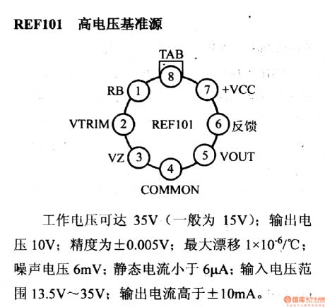
Working voltage of REF 101 high voltage reference source can be as large as 35V(15V in general). The output voltage is 10V, accuracy±0.005V, maximum drift 1×10⁻⁶/℃,noise voltage 6mV, static current lower than 6µA, input voltage range 13.5V~35V and output current higher than ±10mA. (View)
View full Circuit Diagram | Comments | Reading(677)
Regulator DC-DC Circuit and Pin of Power Supply Monitor and its Main Features SH1605A 5A Switched Regulator
Published:2011/9/13 0:13:00 Author:Zoey | Keyword: Regulator, DC-DC Circuit, Pin of Power Supply Monitor, Switched Regulator

The output current of SH1605A 5A switched regulators is 5A, and their output voltage ranges from 3.0V to 3.5V, the working frequency can be adjusted to 150kHz. The maximum voltage input is 40V, with the power of 20W. Working temperature of SH1605ASC is 0~+70℃, and SH1605ASM -55~+125℃. These regulators have interior frequency compensation and have high-speed soft free steering diodes, whose maximum positive current is 8.0A. 1Empty, 2 VREF, 3 Error Amplied Input ,4 CT, 5 Input, 6Empty, 7 Steering Diodes(Positive), 8 Output, frame ground.
(View)
View full Circuit Diagram | Comments | Reading(671)
Regulator DC-DC Circuit and Pin of Power Supply Monitor and its Main Features TA78DLOOP Regulator
Published:2011/9/13 0:15:00 Author:Zoey | Keyword: Regulator, DC-DC Circuit, Pin of Power Supply Monitor, Main Features

The TA78DLOOP series Three-terminal Regulators (Positive output) can output fixed low-margin voltage, the maximum current output is 250mA, and in a spare state, the typical current will be 500μA. When the current input turns to be 200mA, the minimum margin between output voltage and input voltage is below 0.6V, the maximum input voltage is 29V and the power is 800mW. The working temperature is limited from -40 to +85℃.This circuit itself has interior overcurrent, overtemperature and short circuit- proof devices, as soon as the voltage exceeds 60V, the power supply will be cut off.
(View)
View full Circuit Diagram | Comments | Reading(714)
Regulator DC-DC Circuit and Pin of Power Supply Monitor and its Main Features-MAX641/642/643
Published:2011/9/13 2:37:00 Author:Zoey | Keyword: Regulator, DC-DC Circuit, Boost Converter, COMS

MAX641/642/643 CMOS DC-DC boost converter is a switched inverted regulator, it has a interior MOS FET that has a peak of 325mA, this FET can constitute an inverted DC-DC converter with a fixed 10-W output. Therein, MAX 641 is 5V, MAX642 is 12V and MAX643 is 15V.For this converter, typical efficiency is 80% and outupt voltage error can be 5% or 10% and typical static current is 135µA. When the input voltage reaches 5V,oscillation frequency will be 45kHz and range of input voltage +2.0V~+16.5V. Maximum voltage of VOUT, LX and LBO terminal is 18V. Peak of output current of LX terminal is 325mA, LBO 50mA. If room temperature drops to below 50℃, power of DIP platic encapsulation will be 625mW, micro platic encapsulation will be 450mA, and ceramic encapsulation 800mW. Working temperature range of MAX641C/632C/643C is 0~+70℃, MAX641E/642E/643E -40~+85℃, MAX641M/642M/643M -55~+125℃. This converter has an interior circuit for low input voltage-detection
(View)
View full Circuit Diagram | Comments | Reading(731)
Regulator DC-DC Circuit and Pin of Power Supply Monitor and its Main Features-MAX662
Published:2011/9/13 2:36:00 Author:Zoey | Keyword: Regulator, DC-DC Circuit, Flash Reservoir, Programmable Power Supply

MAX662 refers to Flash reservoir programmable power supply. For MAX 662, the output voltage range is +12V ±5%, output current is 30mA, power is 4.5~5.5V and static current is 320µA. When logically closed, the current of power supply can be limited to 70µA. External capacitance between C1+, C1-, C2+ and C2- is 0.22µF, while between VCC and VOUT connected to the ground is 0.1µF. The working temperature range is 0~+70℃. (View)
View full Circuit Diagram | Comments | Reading(661)
Regulator DC-DC Circuit and MAX663 CMOS Regulator
Published:2011/9/13 2:35:00 Author:Zoey | Keyword: Regulator, DC-DC Circuit,
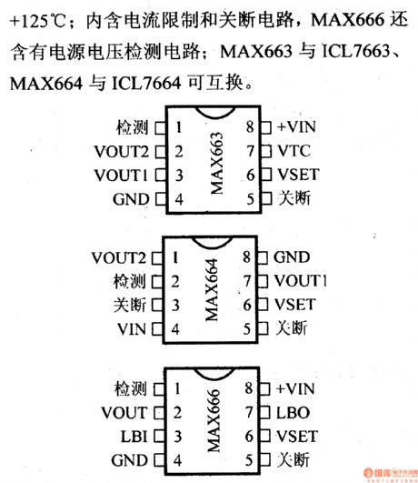
MAX663/666 refers to CMOS positive output regulator, while MAX664 refers to the negative one. If VSET is connected to the ground, output voltage of MAX663/666 will be 5V, and MAX666 will be -5V. If VSET is connected to external resistance, output voltage range of MAX663/666 will be 1.3~16V, and MAX664 will be -1.3~-16V. The output current is 40mA, static current is 12µA. Input voltage range of MAX663/666 is 2~16.5V, MAX664 is -2~-16.5V. Working temperature range of MAX663C/664C/666C is 0~+70℃, MAX663E/664E/666E -40~+85℃, MAX663M/664M/666M -55~+125℃. This regulator has circuits for current-restriction and power-off. MAX666 has a detection circuit for voltage of power supply. (View)
View full Circuit Diagram | Comments | Reading(811)
Regulator DC-DC Circuit and Pin of Power Supply Monitor and its Main Features TA78L00P Regulator
Published:2011/9/13 0:14:00 Author:Zoey | Keyword: Regulator, DC-DC Circuit, Pin of Power Supply Monitor
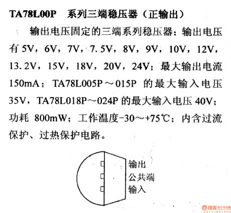
TA78LOOP series Three-terminal Regulator
Three-terminal regulators can output fixed voltage, the voltage can be 5V, 6V, 7V, 7.5V, 8V, 9V, 10V, 12V, 13.2V, 15V, 18V, 20V, 24V. The maximum current output is 150mA, the maximum voltage of TA78L005P~015p is 35V, and TA78L018P~024P is 40V. The power is 800mW and the working temperature is between -30 to +75 ℃. This circuit itself has interior overcurrent and overtemperature proof devices. (View)
View full Circuit Diagram | Comments | Reading(769)
Regulator DC-DC Circuit and Pin of Power Supply Monitor and its Main Features-MAX630
Published:2011/9/13 3:00:00 Author:Zoey | Keyword: Regulator, DC-DC Circuit, COMS, Boost converter
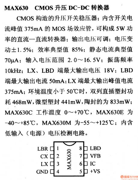
MAX638 CMOS DC-DC boost converter is a switched regulator, it has a interior MOS FET that has a peak of 375mA, this FET can constitute a 5-W DC-DC converter. Its voltage output is adjustable and input volage range is 2.0~16.5V. For this converter, typical efficiency is 85%, voltage variation ±1.5%, typical static current 70µA, oscillation frequency 10kHz. Maximum ouput voltage of LX and LBO terminal is 18V, peak of output current of LX is 375mA, LBO 50mA. If room temperature drops to below 50℃, power of DIP platic encapsulation will be 468mW, micro platic encapsulation will be 441mA, and ceramic encapsulation 833mW. Working temperature range of MAX630C is 0~+70℃, MAX630E -40~+85℃, MAX630M -55~+125℃. This converter has an interior circuit for input voltage-detection.
(View)
View full Circuit Diagram | Comments | Reading(650)
Regulator DC-DC Circuit and Pin of Power Supply Monitor and its Main Features-MAX631
Published:2011/9/13 2:59:00 Author:Zoey | Keyword: Regulator, DC-DC Circuit, CMOS, Boost Converter
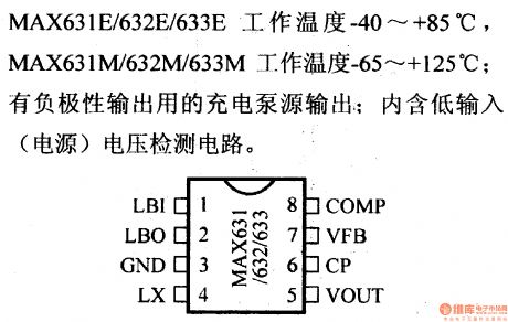
MAX631/632/633 CMOS DC-DC boost converter is a switched regulator, it has a interior MOS FET that has a peak of 325mA, this FET can constitute a DC-DC converter with a fixed output. Therein, MAX 631 5V, MAX632 12Vand MAX633 15V.For this converter, typical efficiency is 80%, typical working current 135µA, output voltage error 5% and 10%, oscillation frequency 45kHz. Maximum voltage of VOUT, LX and LBO terminal is 18V, peak of output current of LX is 325mA, LBO 50mA. If room temperature drops to below 50℃, power of DIP platic encapsulation will be 625mW, micro platic encapsulation will be 450mA, and ceramic encapsulation 800mW. Working temperature range of MAX631C/632C/633C is 0~+70℃, MAX631E/632E/633E -40~+85℃, MAX631M/632M/633M -65~+125℃. This converter has an interior circuit for low input voltage-detection and an output pump for spare negative ouput.
(View)
View full Circuit Diagram | Comments | Reading(768)
SHB6605 Power-Drive Integrated Circuit Diagram
Published:2011/9/13 0:12:00 Author:Zoey | Keyword: SHB6605 Power Drive, Integrated Circuit Diagram
As a power driver IC, SHB6605 is widely used in air conditioners controlled by microcomputers, such as Changhong, Chinese style series air conditioners.1 FeaturesSHB6605 IC consists a power driver circuit, a speed adjustment circuit, and other auxiliary functions circuits. It is typically used to drive the indoor fan motor, for operation of different speeds .2 Pin functions and DataSHB6605 IC pin 13 single in-line package for Changhong KFR-36GW / D air-conditioner , the pin functions of integrated circuit and data have been listed in Table 1
(View)
View full Circuit Diagram | Comments | Reading(1007)
Regulator DC-DC Circuit and Pin of Power Supply Monitor and its Main Features- MAX635/636/637
Published:2011/9/13 2:54:00 Author:Zoey | Keyword: Regulator, DC-DC Circuit, COMS, Boost Converter, Inverted Output
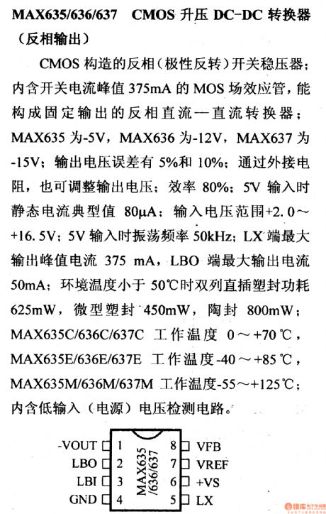
MAX635/636/637 CMOS DC-DC boost converter is a switched inverted regulator, it has a interior MOS FET that has a peak of 375mA, this FET can constitute an inverted DC-DC converter with a fixed output. Therein, MAX 635 -5V, MAX636 -12V and MAX633 -15V.For this converter, typical efficiency is 80%. When the input voltage reaches 5V, typical static current will be 85µA, oscillation frequency 45kHz and range of input voltage +2.0V~+16.5V. Peak of output current of LX terminal is 325mA, LBO 50mA. If room temperature drops to below 50℃, power of DIP platic encapsulation will be 625mW, micro platic encapsulation will be 450mA, and ceramic encapsulation 800mW. Working temperature range of MAX635C/636C/637C is 0~+70℃, MAX635E/636E/637E -40~+85℃, MAX635M/636M/637M -55~+125℃. This converter has an interior circuit for low input voltage-detection
(View)
View full Circuit Diagram | Comments | Reading(705)
Practical Technology Circuit Diagram for Digital Integrated Circuit
Published:2011/9/13 0:11:00 Author:Zoey | Keyword: Practical Technology, Digital, Integrated Circuit
1.Time fordata setup and maintainmentDigital Circuit mainly refers to synchronouscircuits , which means by using a clock, part of the circuit or all circuits can worksynchronously.synchronouscircuits usually adoptD trigger or J-Ktrigger tolatch the data. Using these triggers, we should pay attention to the latched signal and clock timing, if thereis anyproblem, it will cause circuit malfunction. Figure a, b, c refer to the time for data setup ts and maintainment th. Trigger D uses the clock edge to read the data input and output. Before the ascending edge appears, the data should be setup. This time margin is ts. Afer the ascending edge appears, the data needs to be maintained for some time, this time margin is th.The higher IC's working speed, the shorter time is required.
In practical, if ts and th are not long enough, the trigger will be in a multi-valued state, that is, in ameta-stable state,which means theinput processwillhave along delay time, the level will not be determined, and the trigger will havemalfunction.
(View)
View full Circuit Diagram | Comments | Reading(571)
Regulator DC-DC Circuit and Pin of Power Supply Monitor and its Main Features-MAX639
Published:2011/9/13 2:43:00 Author:Zoey | Keyword: Regulator, DC-DC Circuit, Pin, Adjustable Buck regualtor
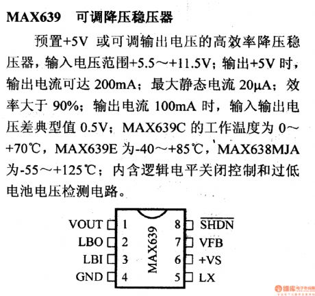
Output voltage (adjustable) range of MAX639 buck regulator is +5.5V~+11.5V. When output voltage reaches +5V, the output current can be 200mA, and maximum static current can be 20µA, efficiency will exceed 90%. If the current is 100mA, typical value of margin between input and ourput voltage will be 0.5V. Working temperature range of MAX639C is 0~+70℃, MAX639E -40~+85℃, MAX638MJA -55~+125℃. This converter has an interior logic level-close controller and a circuit for low voltage detection of the cells. (View)
View full Circuit Diagram | Comments | Reading(707)
| Pages:483/2234 At 20481482483484485486487488489490491492493494495496497498499500Under 20 |
Circuit Categories
power supply circuit
Amplifier Circuit
Basic Circuit
LED and Light Circuit
Sensor Circuit
Signal Processing
Electrical Equipment Circuit
Control Circuit
Remote Control Circuit
A/D-D/A Converter Circuit
Audio Circuit
Measuring and Test Circuit
Communication Circuit
Computer-Related Circuit
555 Circuit
Automotive Circuit
Repairing Circuit