
Circuit Diagram
Index 486
STK392-150、STK392-570 Assembling and Emendation Thick Film Integrated Circuit Diagram
Published:2011/9/13 0:01:00 Author:Zoey | Keyword: Assembling and Emendation , Thick Film , Integrated Circuit Diagram
(View)
View full Circuit Diagram | Comments | Reading(758)
Isolated Data Acquisition System Circuit composed by AD7714 and Microprocessor
Published:2011/9/13 6:48:00 Author:Vicky | Keyword: Isolated Data Acquisition, Microprocessor

The above picture is a isolating data acquisition made up of five-channel low-dissipation programmable sensor signal processor AD7714 and micro-processor. AD7714 is available in low-dissipation narrow-bandwidth, and high-resolution data acquisition system. Three-line serial interface enables the data acquisition system to realize isolating by only three optical couplers. If input signals from AD7714 analog input end are positive, then the whole system canuse a single-power-supply of +3V or +5V. (View)
View full Circuit Diagram | Comments | Reading(1128)
Infrared remote control volume potentiometer (CD4528, CD40193, CD4067)
Published:2011/9/12 21:53:00 Author:Christina | Keyword: Infrared, remote control, volume potentiometer
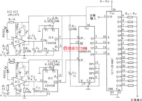
The volume potentiometer is composed of the CMOS digital integrated circuit, and it can be used as the volume control potentiometer of the home audio power amplifier circuit. And it can be used as the voltage regulator of other electrical equipments or instruments. The circuit is as shown in the figure. The full-circuit is composed of the double-channel infrared remote control transmitter, the double-channel infrared receiving signal amplifier, the channel selection and controller, the resistance network and the adding and subtracting controller.
The launch circuit:
The receiving circuit:
(View)
View full Circuit Diagram | Comments | Reading(8481)
The Xiaoshentong XQB20-A washing machine circuit principle diagram
Published:2011/9/12 21:53:00 Author:Christina | Keyword: Xiaoshentong, washing machine, principle diagram

The Xiaoshentong XQB20-A washing machine circuit principle diagram is as shown in the figure:
(View)
View full Circuit Diagram | Comments | Reading(4170)
The voltage-controlled oscillator circuit with high output amplitude stability
Published:2011/9/12 21:52:00 Author:TaoXi | Keyword: Voltage-controlled, oscillator, high, output amplitude, stability

The voltage-controlled oscillator circuit with high output amplitude stability is as shown in the figure. In this circuit, the VT2 controls the collector electrode current of VT1, so the oscillation amplitude of VT1 is very stable. The output signal of VT4 is detected by VD2 to change into the DC signal, it is the automatic gain control working state, so you can make the DC voltage keep constant. The midpoint voltage of RP1 is -0.6V, the current of R1 and R2 can keep the equal, so we can make the output amplitude keep in a constant value. The oscillation frequency is decided by the L1, C2, the capacitance of VD1 and the distributed capacitance.
(View)
View full Circuit Diagram | Comments | Reading(1110)
0M8839PS-K9G216 Digital monolithic small signal processing integrated circuit diagram
Published:2011/9/13 19:47:00 Author:Nancy | Keyword: small signal processing , integrated circuit

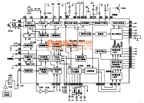
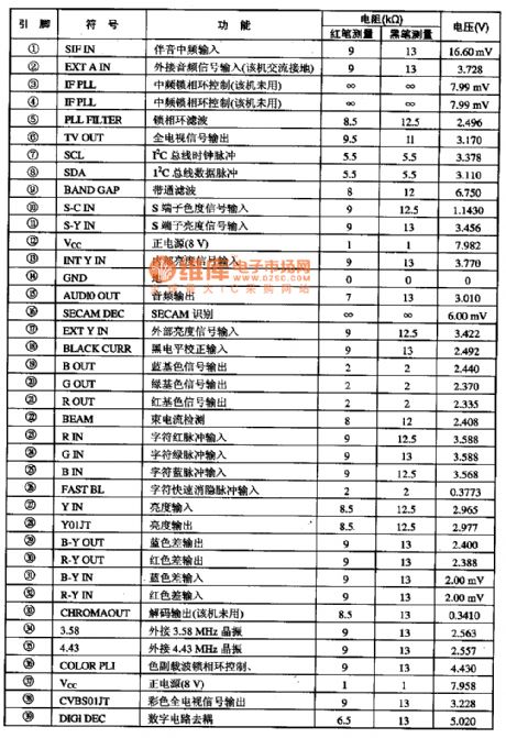
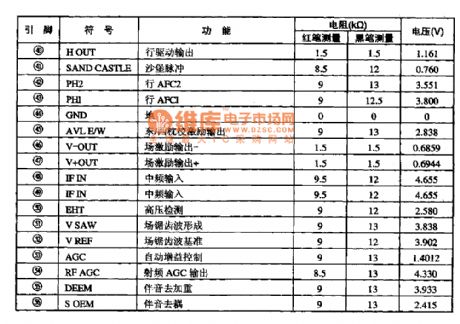
The 0M8839PS-K9G216 is a new generation of monolithic TV V, C, D processing integrated circuit of Philips (a product of the subsidiary in Taiwan). It is widely used in all kinds of a new generation of digital big TV screens.
1. The function and characteristics The 0M8839PS-K9G216 integrated circuit contains a multi system PLL medium frequency demodulation circuit, 4.5-6.5 MHz multi format FM sound intermediate frequency demodulation circuit, self-adjusting PAL/NTSC/SECAM color decoder, 1 line baseband delay line, comb filter, dynamic skin color blue enhance correction circuit, line synchronous controlled by double loop, line/field oscillation and efficient line/field excitation circuitry and east/west pulvinar calibration pulse output and some other units. (View)
View full Circuit Diagram | Comments | Reading(994)
Sequence timer diagram composed by NE555
Published:2011/9/13 19:48:00 Author:Nancy | Keyword: Sequence timer

Figure 1 is the sequence timer diagram composed by NE555. The timer can set time any time when the power is connected, break and control the external system to work. In the circuit, K1-K3 are relays used to control the corresponding system to work, adjust the resistance of the RP1-RP3, which can change the break time of the relay. The pin 2 and 6 of NE555(1) connected together, when the power is connected, if the NE555(1) works, C1 charges instantaneously and the charging current flows through pin 2 to C1. At the same time, a waveform output from the pin 3 of NE555(1) forms a trigger pulse after color processed by the G1, which is added to the pin 2 of NE555(1) and make it work. (View)
View full Circuit Diagram | Comments | Reading(2437)
Square Wave Turning Triangular Wave Circuit
Published:2011/9/12 23:49:00 Author:Sue | Keyword: Square Wave, Triangular Wave

The picture shows the oscillating circuit with triangular wave and square wave output. The circuitconsists of Miller integrator A2 and Schmitt trigger A1, which can generate triangular wave and square wave output.The oscillation frequency is determined by Miller integrator's time constant (R3+R4)C1 and trigger's lagging voltage Vcc(R1+R2)/(R1+R2+R3), and the Vcc is power voltage.By adjusting the resistor R3, the oscillation frequency can be changed. By adjusting the resistor R2, the triangular wave's outputlatitude can be changed and the oscillation frequency can also be changed. (View)
View full Circuit Diagram | Comments | Reading(907)
Retractable Dot Display Level Indicator Composed of SL322
Published:2011/9/12 23:49:00 Author:Sue | Keyword: Retractable, Dot Display, Level Indicator

The picture shows the retractable dot display level indicator circuit. The circuit consists of luminescent display drive SL322, LED D1-D5, transistor BG1-BG5. When K is disconnected, the triodes are all connected to the ground. When the level becomes higher which makes the LED D2 illuminated, B's level becomes higher and BG1 is connected which will make the LED D1 off. When the level becomes higher which makes D3 illuminated, C's level becomes higher which makes BG2 connected, and D2 will be off. At this time, B's level doesn't change and BG1 remains disconnected. D1 is still not illuminated. (View)
View full Circuit Diagram | Comments | Reading(747)
Radio Advertising Voice Circuit
Published:2011/9/12 23:45:00 Author:Felicity | Keyword: Radio Advertising, Voice, Circuit

Work of the circuit
BUSY signal is the Uniquefeatureof the voice chip. We can use it to control the power circuit of the radio.
(View)
View full Circuit Diagram | Comments | Reading(1431)
Anti-toll-fraud circuit diagram
Published:2011/9/7 5:02:00 Author:Vicky | Keyword: Anti-toll-fraud circuit


Anti-toll-fraud circuit is shown in the above picture. The circuit in the picture is a anti-toll-fraud circuit which also performs collinear security feature. It is mainly made up of illegal parallel examine circuit, noise interference circuit, linear privacy-keeping circuit. The circuit is assembled between the telephone device and the exterior line. When there is toll-fraud, the circuit starts working and sends strong noise to the line, which makes the pulse or double audio frequency sent by the toll-fraud unable to be received. Meanwhile, the anti-toll-fraud indication light is lighted, and the host can track the caller. (View)
View full Circuit Diagram | Comments | Reading(1037)
Circuit diagram of controlling groups of light by one single switch
Published:2011/9/7 1:25:00 Author:Vicky | Keyword: controlling, lingt, single switch

As shown in the above circuit diagram, when the power switch K is conducted for the first time, 1# light illumines at once. Because voltage of the capacitor C3 would not change suddenly, the photo-coupler G is conducted only at the moment that switch K is conducted. But soon G stops. In addition, saltation does not occur to the voltage of the capacitance C4, so silicon controlled rectifier S1 would not be conducted (C1 hasn’t generated voltage at the moment of the connection of K, likewise, S2 would not be conducted). Therefore, 2# and 3# light would not lighten. (View)
View full Circuit Diagram | Comments | Reading(1257)
Circuit diagram of electronic code lock with self-locking function
Published:2011/9/7 1:23:00 Author:Vicky | Keyword: electronic code lock , self-locking function


The circuit is shown as in the above picture. Silicon controlled rectifiers SCR5, SCR6, and SCR7 are the main control components of the code lock. If the three-digit number code keys are pressed down in the right sequence (AN2, AN5 and AN7 in this case) , the silicon controlled ractifiers SCR2, SCR3, and SCR4 are conducted in turn, thus to conduct SCR5, SCR6, and SCR7 in turn. VT1 is saturated and conducnted. Electromagnet starts move. Meanwhile, SCR4 is conducted when the AN7 is pressed down, and then VT2 is saturated and conducted, which makes those keys not work then.
(View)
View full Circuit Diagram | Comments | Reading(1695)
Circuit diagram of DC converter from 12V to 24 V
Published:2011/9/7 0:54:00 Author:Vicky | Keyword: DC converter

Different types of voltage value such as 15V, 16V, 18V, 20V, 22V, and 24V etc. can be changed by changing the resistance.
L1 uses a magnetic loop of 2cm and 1.7 polyester varnished wires to wind it closely for 35 turns. And then it is sealed up by silicon rubber, otherwise it is easy to generate sizzling sound.
Meanwhile the direction of the route should be paid attention to, otherwise the sizzling sound will also occurand the field-effect tube emits heat and destroys due to the self-excitation caused by routing problem. If possible, paster component of UC3843 can also be used.
L2 can use the magnetic loop of old energy-saving light to wind closely. There is no special requirement.
(View)
View full Circuit Diagram | Comments | Reading(7263)
Circuit diagram of multi-vibrator composed by triodes
Published:2011/9/7 3:48:00 Author:Vicky | Keyword: multi-vibrator, triode


The above picture is a multi-vibrator composed by triodes. The circuit is still composed of phase inverter coupling by two-polar base resistance-capacity. When the circuit power is on, the two tubes cannot be conducted at once, because the charging route for CA is: Ec→R2→CA→Rc1; the charging route for CB is : Ec→Rc2→CB→R1. When CA and CB are charged to a certain value, UCA and UCB , as the forward bias voltage of tube base loop, make Ib1 and Ib2 increase. Due to the performance of positive feedback, the BG1 and BG2 soon becomes saturation. This is a temporarily-stable state.
Once the saturation starts, CA discharges via emitter framework of Rb2, BG2 and resistance Rc1. (View)
View full Circuit Diagram | Comments | Reading(975)
MAX1576 high-power white LED driver circuit diagram
Published:2011/9/12 19:58:00 Author:Lucas | Keyword: high-power, white LED driver
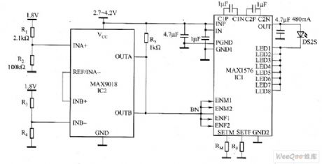
The circuit includes the charge pump regulator (IC1) which is suitable for camera flash applications, and the device can provide current regulation for 8 white LEDs. The LED1 ~ LED8 connected in parallel can provide 480mA current for a single IW, LUXE * tar high-power white LED module. When open drain input (ENM1/ENM2 or ENF1/ENF2) is pulled to ground, IC1 gets into shutdown mode. The circuit uses a thermistor (R2) and dual open-drain comparator (IC2) with internal reference to constitute a compact space and very low-cost thermal shutdown circuit.
(View)
View full Circuit Diagram | Comments | Reading(1391)
reference voltage circuit composed by LM4130
Published:2011/8/25 7:43:00 Author:Nancy | Keyword: reference voltage

The reference voltage circuit composed by LM4130 is shown as the figure. In the circuit, the temperature controller formed by A1~A4 makes the junction temperature of LM3140 keep at 75 ℃ and the external temperature of LM3140 change between 85 and 40 ℃, and the range is 125 ℃, but the internal temperature is 85 and 40 ℃, the range is narrower 6.25 times than that of external temperature, which make the temperature coefficient of the output reference voltage of LM4130 improved significantly.
The thermostat is formed by the LM4130 chip surface, and the empty pins (pin 1 and 3) used to adjust the temperature coefficient become a part of the temperature control loop, so the thermostat doesn't use heat shield, and has no special requirements to the mechanical device and heater. In addition, all the components can be installed in surface, and the space requirement to the substrate is least. (View)
View full Circuit Diagram | Comments | Reading(1253)
Repeat timing circuit formed by PUT
Published:2011/8/25 7:42:00 Author:Nancy | Keyword: PUT, repeat timing circuit
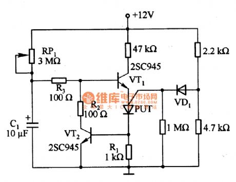
Figure 1 is the repeat timing circuit formed by PUT. It is a repeat timing circuit composed by one PUT, two transistors and a diode, which is not effected by the change of the the power supply voltage and the temperature and has long-term stability. When PUT conducts, the anode current is shunted by the transistor VT2, the base current of VT1 is cut off and the PUT resets. The negative temperature coefficient of VD1 makes a temperature compensation to the offset voltage of PUT. The RP1 resistance is larger, which is 3 MΩ, so we should choose the gold/film resistor with small temperature effect and C1 selects a knob capacitor with small leakage current. (View)
View full Circuit Diagram | Comments | Reading(759)
HA1392 audio power amplifier circuit diagram
Published:2011/8/25 7:41:00 Author:Nancy | Keyword: audio, power amplifier

The circuit is shown as above, IC1 and T1, IC2 and T2 form the current negative feedback absorption constant current source respectively, which are the voltage,the current transition and amplification of the the positive half cycle and negative half cycle of the audio signal, which makes that the base current of T3 and T4 is only controlled by the input voltage of IC1 and IC2, in other words, once the the op-amp input is a constant voltage value, the current which flows throught the collector current of the final stage transistor is also a constant value.The W1, W2 (multiturn potentiometer) are respectively used to adjust the static current and output zero of T3 and T4, and the IC3 and R1, R2, R5 form the quasi current negative circuit, as long as you change the corresponding resistance value of R3, R4 or R2, R6, you can change the value of the gain. (View)
View full Circuit Diagram | Comments | Reading(3356)
TDA1514 (40W+40W)amplifier circuit
Published:2011/8/25 7:41:00 Author:Nancy | Keyword: amplifier

The TDA1514 is a sound special circuit designed to adapt to the high fidelity requirement of power amplifier for the digital sound, which is a 9-pin mono channel power amplifier integrated circuit with single package structure. Because of the use of advanced integration technology, the TDA1514 has some distinctive characteristics such as high output power, small distortion, wide frequency response and reliable performance etc.The TDA1514 is built with internal overheating protection and on-off noise suppression function, the static noise time is decided by an external circuit. (View)
View full Circuit Diagram | Comments | Reading(5650)
| Pages:486/2234 At 20481482483484485486487488489490491492493494495496497498499500Under 20 |
Circuit Categories
power supply circuit
Amplifier Circuit
Basic Circuit
LED and Light Circuit
Sensor Circuit
Signal Processing
Electrical Equipment Circuit
Control Circuit
Remote Control Circuit
A/D-D/A Converter Circuit
Audio Circuit
Measuring and Test Circuit
Communication Circuit
Computer-Related Circuit
555 Circuit
Automotive Circuit
Repairing Circuit