Basic Circuit
Repeat timing circuit formed by PUT
Published:2011/8/25 7:42:00 Author:Nancy | Keyword: PUT, repeat timing circuit | From:SeekIC

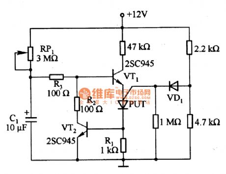
Figure 1 is the repeat timing circuit formed by PUT. It is a repeat timing circuit composed by one PUT, two transistors and a diode, which is not effected by the change of the the power supply voltage and the temperature and has long-term stability. When PUT conducts, the anode current is shunted by the transistor VT2, the base current of VT1 is cut off and the PUT resets. The negative temperature coefficient of VD1 makes a temperature compensation to the offset voltage of PUT. The RP1 resistance is larger, which is 3 MΩ, so we should choose the gold/film resistor with small temperature effect and C1 selects a knob capacitor with small leakage current.
Reprinted Url Of This Article:
http://www.seekic.com/circuit_diagram/Basic_Circuit/Repeat_timing_circuit_formed_by_PUT.html
Print this Page | Comments | Reading(3)

Article Categories
power supply circuit
Amplifier Circuit
Basic Circuit
LED and Light Circuit
Sensor Circuit
Signal Processing
Electrical Equipment Circuit
Control Circuit
Remote Control Circuit
A/D-D/A Converter Circuit
Audio Circuit
Measuring and Test Circuit
Communication Circuit
Computer-Related Circuit
555 Circuit
Automotive Circuit
Repairing Circuit
Code: