
Circuit Diagram
Index 1335
OVERTONE_CRYSTAL_OSCILLATOR
Published:2009/6/24 20:49:00 Author:Jessie

The crystal element in this circuit is con-nected directly between the base and ground.Capacitor C1 is used to improve the feedback due to the internal capacitances of the transis-tor. This capacitor should be mounted as close as possible to the case of the transistor. The LC tank circuit in the collector of the transistor is tuned to the overtone frequency of the crystal.The emitter resistor capacitor must have a capacitive reactance of approximately 90 ohms at the frequency of operation. The tap on induc-tor L1 is used to match the impedance of the collector of the transistor. In most cases, the optimum placement of this tap is approximately one-third from the cold end of the coil. The placement of this tap is a trade-off between stability and maximum power output. The out-put signal is taken from a link coupling coil, L2, and operates by transformer action. (View)
View full Circuit Diagram | Comments | Reading(1926)
HIGH_FREQUENCY_CRYSTAL_OSCILLATOR
Published:2009/6/24 20:42:00 Author:Jessie
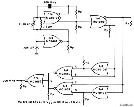
Circuit NotesOne section of the MC10101 is connected as a 100 MHz crystal oscillator with the crystal in series with the feedback loop. The LO tank circuit tunes the 100 MHz harmonic of the crystal and may be used to calibrate the circuit to the exact frequency. A second section of the MC10101 buffers the crystal oscillator and gives complementary 100 MHz signals. Thefrequency doubler consists of two MC10101 gates as phase shifters and two MC1662 NOR gates. For a 50% duty cycle at the output, the delay to the true and complement 100 MHz signals should be 90'. This may be built pre-cisely with 2.5 ns delay lines for the 200 MHz output or approximated by the two MC10101 gates as shown. (View)
View full Circuit Diagram | Comments | Reading(1444)
THIRD_ORDER_BUTTERWORTH_CROSSOVER_NETWORK
Published:2009/6/24 20:38:00 Author:Jessie

View full Circuit Diagram | Comments | Reading(1042)
ASYMMETRICAL_THIRD_ORDER_BUTTERWORTH_ACTIVE_CROSSOVER_NETWORK
Published:2009/6/24 20:38:00 Author:Jessie

View full Circuit Diagram | Comments | Reading(1104)
ACTIVE_CROSSOVER_NETWORK
Published:2009/6/24 20:36:00 Author:Jessie

View full Circuit Diagram | Comments | Reading(1230)
LOW_FREQUENCY_RELAY_OSCILLATOR
Published:2009/6/24 5:42:00 Author:Jessie

Depending on the value of C and the resistance of the relay coil, and the difference in pull-in and drop-out voltage, this circuit will oscillate at a low frequency. R limits in rush current to capacitor C to a level that the relay contacts can handle. Typically, for a 400-Ω relay, R can be 20 to 440 ohms.Flash rate is approximately 1 cycle/second, depending on the relay. (View)
View full Circuit Diagram | Comments | Reading(2541)
MOMENTARY_RELAY_CIRCUIT
Published:2009/6/24 5:33:00 Author:May

The charging current of a capacitor can be used if a momentary relay-on circuit is needed Depending fin the relay characteristics,C will vary from 1000 to 4000 μF or so for a 1-s hold time if a 500-Ω relay is used.RD discharges capacitor C to reads,the circuit for the next oPeration The valueshould be high enoughso as notto maintian the relay closure at highest expected supply voltage. (View)
View full Circuit Diagram | Comments | Reading(2790)
LATCHING_RELAY_ALARM_CIRCUIT
Published:2009/6/24 5:30:00 Author:May

Momentarily closing any sensors will cause K1 to latch. S1 must be depressed to reset circuit. If any sensor is still closed circuit will not reset. (View)
View full Circuit Diagram | Comments | Reading(1265)
5_TO_33_V_SURFACE_MOUNT_SWITCHING_REGULATOR
Published:2009/6/24 5:29:00 Author:May

This converter provides 3.3 V at 150 mA from an input voltage of 5 V. Peak inductor current is limited to 340 mA by connecting pin 6 (IPGM) to ground. For applications requiring higher output current, connect pin 6 to Vin. Under this condition, the maximum load current is increased to 425 mA. (View)
View full Circuit Diagram | Comments | Reading(578)
POSITIVE_REGULATOR_SINKS_CURRENT
Published:2009/6/24 5:28:00 Author:May

Generally speaking, conventional positive voltage regulators can only source current; they can't sink it. However, the positive regulator shown breaks that rule because it can perform both functions.The idea is to have the control transistor Q1 in shunt so that the regulator can either source or sink current.The circuit provides +3-V output from a +5-V supply. U1 is a bandgap reference that supplies a stable +2.5-V reference to the error amplifier (A1). The output voltage (VO) is sampled by the resis-tor network (R1 and R2). If VO were to increase, A1 will drive the base of Q1 harder, increasing the collector current (IC).This increases the drop across R3 and VO decreases, thus regulating the output voltage. The output voltage is givenby VO = 2.5(1 + R1/R2)Under no load conditions, Q1 draws 110 mA [(Vin-VO)/R3]. With a load connected, and as the regulator begins to source load current (IL), IC decreases to keep the drop across R3 constant.At IL 100 mA, Q1 carries 10 mA. If RL is connected to the positive supply higher than VO, then the regulator must sink current, and IL becomes negative. At IL = -100 mA, Q1 carries 210 mA while maintaining the output voltage at +3 V. The output voltage will remain constant at +3 V—even if the load current changes sign.With the proper heatsink on Q1, the regulator can sink more than 300 mA. If a sink only option is desired, the dissipation in Q1 can be reduced by using a 180-Ω resistor for R3. R4 limits the base current drive for Q1 and prevents the output of A1 from being clamped at 2 VBE. (View)
View full Circuit Diagram | Comments | Reading(878)
SIMPLE_NOISE_LIMITER
Published:2009/6/24 5:25:00 Author:May

This circuit uses a symmetrical limiter obtained by biasing a transistor to a Q point that is half of the supply voltage and driving it into saturation and cutoff. An input of 1 to 2 V RMS is sufficient. This output will be approximately 4Vp-p into a high-impedance load. (View)
View full Circuit Diagram | Comments | Reading(980)
ADJUSTABLE_NOISE_CLIPPER
Published:2009/6/24 5:22:00 Author:May

This circuit uses two diodes and is a peak-to-peak limiter. The capacitors charge up to a dc level determined by the peak-to-peak audio signal and the clipping control. A positive or negative peak or spike is clipped if it exceeds this level plus the diode drops. The circuit should be operated at several volts level for best results. (View)
View full Circuit Diagram | Comments | Reading(3816)
LOW_DROPOUT_REGULATOR
Published:2009/6/24 5:22:00 Author:May

This low-dropout reference produces a 4.5-V output from a supply just a few hundred mV loading, With 1-mA dc loading,it maintains a stable 4.5-V output for inputs down to 4.7 V. (View)
View full Circuit Diagram | Comments | Reading(0)
AUDIO_NOISE_BASED_VOTING_CIRCUIT
Published:2009/6/24 5:21:00 Author:May

The purpose of this circuit is the selection of the output of two receivers, tuned to the same channel, that has the better signal to noise ratio. This circuit compares the two noise leads from the receivers and selects the one with the lower audio noise level. (View)
View full Circuit Diagram | Comments | Reading(667)
LOW_DROPOUT_THREE_TERMINAL_REGULATORS_FOR_NEW_MICROPROCESSOR_APPLICATIONS
Published:2009/6/24 5:20:00 Author:May

The LT1584/LT1585/LTL1587 are high-perf ormance, low-dropout regulators designed to meet the demands of the newest high speed, low voltage microprocessors. These devices are designed to regulate from 5-V supplies to output voltages between 1.25 V and 3.6 V. The LT1584 can provide up to 7 A of current, making it ideal for powerful Pentium processor or similar applications. The LT1585 can supply up to 4 A, while the LT1587 supplies up to 3 A. The excellent transient response capabil-tty allows thent to maintain good regulation even with significant load steps. Fixed 3.3 V, 3.45 V, 3.6 V and adjustable output voltages are available. (View)
View full Circuit Diagram | Comments | Reading(1225)
REDUCING_RIPPLE_IN_A_SWITCHING_VOLTAGE_REGULATOR
Published:2009/6/24 5:17:00 Author:May

Simple additional circuitry that consists of relatively small components can reduce the output ripple by a factor of about 10. The additional components are indicated by the dashed lines.A current opposing the ripple is injected into the filter capacitor. The essence of the present technique is to inject, into this capacitor, a cur-rent opposite to that which already flows into this capacitor. A small additional winding, L1, in inductor L0 provides transformer coupling to generate the current that opposes the original ripple current. The circuit from L1 through C0 is completed by a small additional extemal inductor L2 and coupling capacitor C1. (View)
View full Circuit Diagram | Comments | Reading(493)
LOW_NOISE_REGULATOR(5_TO_33_V)
Published:2009/6/24 5:16:00 Author:May

In some applications, it is important not to introduce any switching noise within the audio frequency range. To circumvent this problem, a feed-forward capacitor can be used to shift the noise spectrum up and out of the audio band with C2 being the feed-forward capacitor. The peak-to-peak output ripple is reduced to 30 mV over the entire load range. A toroidal surface mount inductor L1 is chosen for its excellent self-shielding properties. (View)
View full Circuit Diagram | Comments | Reading(505)
DUAL_OUTPUT_REGULATOR
Published:2009/6/24 5:14:00 Author:May

If load can go to zero, an optional preload of 1 to 5 kΩ can be used to improve regulation. Many modern circuit designs still need a dual polarity supply. Communication and data acquisition are typical areas where both 5 V and -5 V are needed for some of the IC chips.The current mode architecture and saturating switch design allow the LT1376 to deliver up to 1.5-A load current from the 8-pin SO package. L1 is a 10-μH surface-mount inductor from Coiltronics. The second winding is used to create a negative-output SEPIC (Single-Ended Primary Inductance Converter) topoLogy using D3, C4, C5, and the second half of F1. This converter takes advantage of the fact that the switching signal driving L1 as a positive buck converter is already the correct amplitude for driving a -5-V SEPIC converter. During switch-off time, the voltage across L is equal to the 5-V output plus the forward voltage of D1. An identical voltage is generated in the sec-ond winding, which is connected to generate -5 V using D3 and C5. Without C4, this would be a simple flyback winding connection with modest regulation. The addition of C4 creates the SEPIC topology. Note that the voltages swing at both ends of C4 is theoretically identical-even without the capacitor. The undotted end of both windings goes to a zero ac voltage node, so the equal windings will have equal voltages at the opposing ends. Unfortunately, coupling between windings is never perfect, and load regulation at the negative output suffers as a result. The addition of C4 forces the wind-ing potentials to be equal and (View)
View full Circuit Diagram | Comments | Reading(693)
DOLBΥ_NOISE_REDUCTION_CIRCUIT
Published:2009/6/24 5:14:00 Author:May

View full Circuit Diagram | Comments | Reading(598)
NOISE_GENERATOR
Published:2009/6/24 5:12:00 Author:May

This noise generator uses a Zener diode. The transistors are part of the LM389. (View)
View full Circuit Diagram | Comments | Reading(0)
| Pages:1335/2234 At 2013211322132313241325132613271328132913301331133213331334133513361337133813391340Under 20 |
Circuit Categories
power supply circuit
Amplifier Circuit
Basic Circuit
LED and Light Circuit
Sensor Circuit
Signal Processing
Electrical Equipment Circuit
Control Circuit
Remote Control Circuit
A/D-D/A Converter Circuit
Audio Circuit
Measuring and Test Circuit
Communication Circuit
Computer-Related Circuit
555 Circuit
Automotive Circuit
Repairing Circuit