
Circuit Diagram
Index 1332
TOUCH_SWITCH
Published:2009/6/24 21:10:00 Author:May

Two NAND Schmitt triggers are used as a flip-flop to produce a bridged touch switch. (View)
View full Circuit Diagram | Comments | Reading(0)
CAPACITIVE_SENSOR_SYSTEM
Published:2009/6/24 21:08:00 Author:May

This figure illustrates the electric-field configuration of a capacitive proximity sensor of the ca-paciflector type. It includes a sensing electrode driven by an alternating voltage, which gives rise to an electric field in the vicinity of the electrode; an object that enters the electric field can be de-tected by its effect on the capacitance between the sensing electrode and electrical ground.Also, it includes a shielding electrode (in this case, driven shield 1), which is excited via a volt-age follower at the same voltage as that applied to the sensing electrode to concentrate more of the electric outward from the sensing electrode, increasing the sensitivity and range of the sensor. Be-cause the shielding electrode is driven via a voltage follower, it does not present a significant elec-trical load to the source of the alternating voltage.In this case, the layered electrode structure also includes a reference electrode adjacent to ground, plus a second shielding electrode (driven shield 2), which is excited via a voltage follower at the same voltage as that applied to the reference electrode. Driven shield 2 isolates the reference electrode from the electric field generated by driven shield 1 and the sensing electrode so that a nearby object exerts no ca[acitive effect on the reference electrode.The excitation is supplied by a crystal-controlled oscillator and applied to the sensing and ref-erence electrodes via a bridge circuit. Fixed capacitors C1 and C2 (or, alternatively, fixed resistors RI and R2) are chosen to balance the bridge; that is, to make the magnitude of the voltage at sens-ing-electrode node S equal the magnitude of the voltage at reference-electrode node R.The voltages at S and R are peak-detected and fed to a differential amplifier, which puts out volt-age 7, proportional to the difference between them. When no object intrudes into the electric field of the sensing electrode, the bridge remains in balance, and Vu - 0. When an object intrudes, it changes CS, unbalances the bridge, and causes Vu to differ from zero. The closer the object comes to the sensing electrode, the larger (Vu) becomes.An additional output voltage KVr is available, where K is the amplification and Vr is the voltage on the reference electrode. (View)
View full Circuit Diagram | Comments | Reading(0)
PRECISION_LF_OSCILLATOR
Published:2009/6/24 21:07:00 Author:May

Using R1, R7, and D1 to preset C1 to one third of the supply voltage, this circuit avoids a longer first cycle period than subsequent cycles. (View)
View full Circuit Diagram | Comments | Reading(0)
GATED_1_kHz_OSCILLATOR(NORMALLY_ON)
Published:2009/6/24 21:06:00 Author:May

This gated 1-kHz oscillator offers press-to-turn-off' operation, A, and waveforms at the out-put of pin 3 and across C1, B. (View)
View full Circuit Diagram | Comments | Reading(0)
SIMPLE_TIMED_TOUCH_SWITCH
Published:2009/6/24 21:06:00 Author:May

This circuit produces an output for a time approximately equal to time constant R3/C1.
IC1,IC2 CD4011 quad NAND gateIC3 CD4066 quad bilateral switchC1 47-μF, 25-V electrolytic capacitorC2 100-μF, 25-V electrolytic capacitorC3 220-μF, 25-V electrolytic capacitorC4470-μF, 25-V electrolytic capacitorC5,C6,C7 0.1-μF capacitorRI,R3,R4,R6100-kΩ,1/4-W 5% resistorR7,R9,R10,R12 100-kΩ,1/4-W 5% resistorR2,R5,R8,R11 (View)
View full Circuit Diagram | Comments | Reading(0)
GATED_1_kHz_OSCILLATOR(NORMALLY_OFF)
Published:2009/6/24 21:05:00 Author:May

This gated 1-kHz oscillator offers press-to-turn-on operation, A, and waveforms at the out-put of pin3 and across C1, B. (View)
View full Circuit Diagram | Comments | Reading(0)
TTL_OSCILLATOR_FOR_1_MHz_10_MHz
Published:2009/6/24 21:01:00 Author:May
View full Circuit Diagram | Comments | Reading(0)
96_MHz_CRYSTAL_OSCILLATOR
Published:2009/6/24 21:00:00 Author:May


Circuit NotesBy usmg a crystal between 27.5 and 33 MHz,the 3rd harmonic will deliver between82.5 and 99 MHz. (View)
View full Circuit Diagram | Comments | Reading(0)
LOW_DRIFT_SAMPLE_AND_HOLD
Published:2009/6/24 20:59:00 Author:May

View full Circuit Diagram | Comments | Reading(0)
CRYSTAL_CHECKER
Published:2009/6/24 20:59:00 Author:May

Use this circuit for checking fundamental HF crystals on a 'Go-No-Go' basis. An untuned Colpitts oscillator drives a voltage multiplier rectifier and a current amplifier. If the crystal oscillates, Q2 conducts and the LED lights. A3 or 6V, 40mA bulb could be substituted for the LED. (View)
View full Circuit Diagram | Comments | Reading(0)
1IONIZATION_CHAMBER_SMOKE_DETECTOR
Published:2009/6/24 21:20:00 Author:Jessie
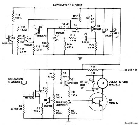
If the smoke alarm signal must be a continuous one rather than pulsating, then the slightly less expensive, all discrete transistor version of the MC14572 may be used. (View)
View full Circuit Diagram | Comments | Reading(2632)
MICROPOWER_4_CHANNEL_SAMPLE_AND_HOLD_CIRCUIT
Published:2009/6/24 20:59:00 Author:May

Three Maxim ICs make up this sample-and-hold circuit. The supply current is only 6μA. (View)
View full Circuit Diagram | Comments | Reading(0)
OVERTONE_CRYSTAL_OSCILLATOR
Published:2009/6/24 20:49:00 Author:May

The crystal element in this circuit is con-nected directly between the base and ground.Capacitor C1 is used to improve the feedback due to the internal capacitances of the transis-tor. This capacitor should be mounted as close as possible to the case of the transistor. The LC tank circuit in the collector of the transistor is tuned to the overtone frequency of the crystal.The emitter resistor capacitor must have a capacitive reactance of approximately 90 ohms at the frequency of operation. The tap on induc-tor L1 is used to match the impedance of the collector of the transistor. In most cases, the optimum placement of this tap is approximately one-third from the cold end of the coil. The placement of this tap is a trade-off between stability and maximum power output. The out-put signal is taken from a link coupling coil, L2, and operates by transformer action. (View)
View full Circuit Diagram | Comments | Reading(0)
WIRELESS_MICROPHONE
Published:2009/6/24 21:20:00 Author:Jessie

An op-amp IC (741) amplifies the audio signal from MIC1, and R12 controls its gain. Audio is fed to the oscillator circuit Q1 and related components. D2 is a varactor diode. Audio fed to D2 causes FM of the oscillator signal. L1 is 1/2 turns of #18 wire on a He diameter form. The antenna is a 12 whip. (View)
View full Circuit Diagram | Comments | Reading(3)
HIGH_FREQUENCY_CRYSTAL_OSCILLATOR
Published:2009/6/24 20:42:00 Author:May
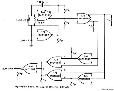
Circuit NotesOne section of the MC10101 is connected as a 100 MHz crystal oscillator with the crystal in series with the feedback loop. The LO tank circuit tunes the 100 MHz harmonic of the crystal and may be used to calibrate the circuit to the exact frequency. A second section of the MC10101 buffers the crystal oscillator and gives complementary 100 MHz signals. Thefrequency doubler consists of two MC10101 gates as phase shifters and two MC1662 NOR gates. For a 50% duty cycle at the output, the delay to the true and complement 100 MHz signals should be 90'. This may be built pre-cisely with 2.5 ns delay lines for the 200 MHz output or approximated by the two MC10101 gates as shown. (View)
View full Circuit Diagram | Comments | Reading(0)
MICRO_TV_TRANSMITTER
Published:2009/6/24 21:19:00 Author:Jessie

For very low power noncritical applications, this small TV modulator can be useful as a shortrange (50 feet) transmitter for video signals. A small camera module can be used as a source. R11 is used to vary dc offset of the modulator. (View)
View full Circuit Diagram | Comments | Reading(2647)
THIRD_ORDER_BUTTERWORTH_CROSSOVER_NETWORK
Published:2009/6/24 20:38:00 Author:May

View full Circuit Diagram | Comments | Reading(0)
LOCAL_OSCILLATOR_FOR_DOUBLE_BALANCED_MIXERS
Published:2009/6/24 21:19:00 Author:Jessie
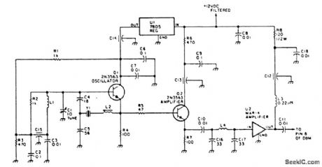
This circuit has an amplifier to supply +10 dBm to an SBL series (Mini-circuits) or similar type doubly-balanced mixer assembly. This circuit has values shown for =80- to 90-MHz crystals, although values of oscillator circuit constants can be scaled for higher or lower frequencies. (View)
View full Circuit Diagram | Comments | Reading(1481)
ASYMMETRICAL_THIRD_ORDER_BUTTERWORTH_ACTIVE_CROSSOVER_NETWORK
Published:2009/6/24 20:38:00 Author:May

View full Circuit Diagram | Comments | Reading(0)
ACTIVE_CROSSOVER_NETWORK
Published:2009/6/24 20:36:00 Author:May

View full Circuit Diagram | Comments | Reading(0)
| Pages:1332/2234 At 2013211322132313241325132613271328132913301331133213331334133513361337133813391340Under 20 |
Circuit Categories
power supply circuit
Amplifier Circuit
Basic Circuit
LED and Light Circuit
Sensor Circuit
Signal Processing
Electrical Equipment Circuit
Control Circuit
Remote Control Circuit
A/D-D/A Converter Circuit
Audio Circuit
Measuring and Test Circuit
Communication Circuit
Computer-Related Circuit
555 Circuit
Automotive Circuit
Repairing Circuit