Digital Circuit
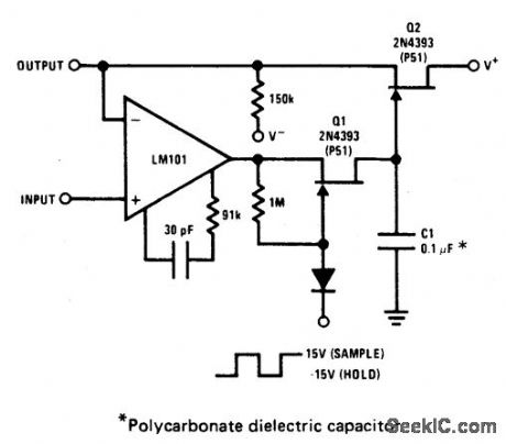
LOW_DRIFT_SAMPLE_AND_HOLD
Published:2009/6/30 3:22:00 Author:May | From:SeekIC

TheJFETs, Q1 and Q2, provide complete buffering to C1, the sample and hold capacitor.During sample, Q1 is turned on and provides a path, rds(on), for charging C1. During hold, Q1 is turned off, thus leaving Q1 ID(off) (<100 pA) and Q2 IGSS (< 100 pA) as the only discharge paths. Q2 serves a buffering function so feedback to the LM101 and output current are supplied from its source.
Reprinted Url Of This Article:
http://www.seekic.com/circuit_diagram/Basic_Circuit/Digital_Circuit/LOW_DRIFT_SAMPLE_AND_HOLD.html
Print this Page | Comments | Reading(3)

Article Categories
power supply circuit
Amplifier Circuit
Basic Circuit
LED and Light Circuit
Sensor Circuit
Signal Processing
Electrical Equipment Circuit
Control Circuit
Remote Control Circuit
A/D-D/A Converter Circuit
Audio Circuit
Measuring and Test Circuit
Communication Circuit
Computer-Related Circuit
555 Circuit
Automotive Circuit
Repairing Circuit
Code: