
Circuit Diagram
Index 1326
ac_VOLTEMTER_HAS_UNIQUE_FEATURES
Published:2009/6/24 22:06:00 Author:May


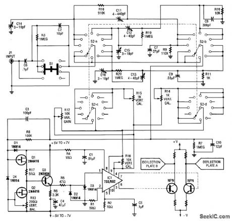
Though it's built with standard components, this ac voltmeter contains many features not typi-cally found in commercial meters; the most unusual is a selection of rectification modes. The meter responses available include true RMS ('fRMS), average, RMS-calibrated average responding, positive peak, negative peak, positive-peak hold, and negative-peak hold.High- and low-pass filters (S1 and S6, respectively) allow the -3-dB-passband to be varied from as little as 10 Hz to 200 Hz, to as wide as dc to 500 kHz. The low-pass filter also is effective in the 100x amplifier mode, where the input equivalent noise level is only 0.3 pV, with 10-kHz roll-off.
(View)
View full Circuit Diagram | Comments | Reading(3438)
VOLTAGE_MONITOR
Published:2009/6/24 22:04:00 Author:May
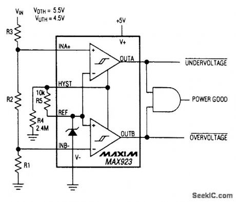
A MAX923 dual comparator is used as a window detector, For a threshold of 4.5V and 5.5V, R1=1.068MΩ, R2=61.9kΩ and R3=1MΩ (View)
View full Circuit Diagram | Comments | Reading(0)
METER_AMPLIFIER_FOR_15_V_SUPPLY
Published:2009/6/24 22:04:00 Author:May
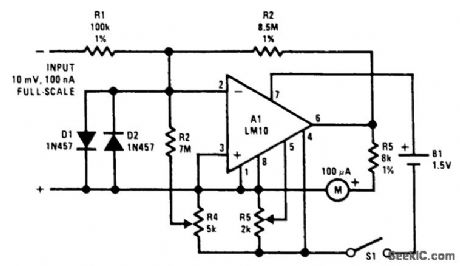
Art LM10 is used as a meter amplifier. Accuracy can be maintained over a 15℃ to 55℃ range for a full-scale sensitivity of 10 mV and 100 nA. The offset voltage error is nulled with R5, and the bias current can be balanced out with R4. The zeroing circuits operate from the reference output and are essentially unaffected by changes in battery voltage, so frequent adjustments should not be neces-sary. Total current drain is under 0.5 mA, giving an approximate life of 3 to 6 months with an AA cell and over a year with a D cell. With these lifetimes, an ON/OFF switch might be unnecessary. A test switch that converts to a battery-test mode might be of greater value. (View)
View full Circuit Diagram | Comments | Reading(580)
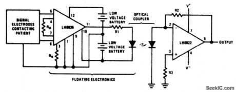
ISOLATION_AMPLIFIER_FOR_MEDICAL_TELEMETRY
Published:2009/6/24 22:02:00 Author:May
View full Circuit Diagram | Comments | Reading(511)
2INSTRUMENTATION_AMPLIFIER
Published:2009/6/24 22:02:00 Author:May

Three-amplifier circuit consumes only 135μW of power from a ±1.5 V power supply.With a gain of 101, the instrumentation amplifier is ideal in sensor interface and biomedical preamplifier applications. The first stage provides all of the gain while the second stage is used to provide common mode rejection and double-ended to single-ended conversion. (View)
View full Circuit Diagram | Comments | Reading(0)
12_V_BATTERY_CHARGER_CONTROL_20_AMPS_RMS_MAX
Published:2009/6/24 22:01:00 Author:May

View full Circuit Diagram | Comments | Reading(985)
SIMPLE_NI_CAD_BATTERY_CHARGER
Published:2009/6/24 22:00:00 Author:May

This circuit provides an adjustable output voltage up to 35 Vdc and maximum output current of 50 mA. Transistor Q1 dissipates quite a bit of heat and must be mounted on a heatsink. (View)
View full Circuit Diagram | Comments | Reading(595)
VOLTAGE_CONTROLLED_TWO_PHASE_OSCILLATOR
Published:2009/6/24 22:00:00 Author:May
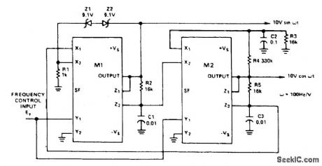
This circuit uses two multipliers for integration-with-contro llable-time -constants in a feedback loop. R2 and R5 will be recognized in the AD534 voltage-to-current configuration; the currents are integrated in C1 and C3, and the voltages they develop are connected at high impedance in proper polarity to the X inputs of the next AD534. The frequency-control input, EY, varies the integrator gains, with a sensitivity of 100 Hz/V, and frequency error typically less than 0.1% of full scale from 0.1V to 10V (10 Hz to 1 kHz). C2 (proportional to C1 and C3), R3, R4 provide regenerative darnp-ing to start and maintain oscillation. Z1 and Z2 stabilize the amplitude at low distortion by degenera-tive damping above ±10V. (View)
View full Circuit Diagram | Comments | Reading(582)
12_V_BATTERY_CHARGER
Published:2009/6/24 22:00:00 Author:May

This circuit is a high performance charger for gelled electrolyte lead-acid batteries. Charger quickly recharges battery and shuts off at full charge. Initially, charging current is limited to 2A. As the battery voltage rises, current to the battery decreases, and when the current has decreased to 150 mA, the charger switches to a lower float voltage preventing overcharge. When the start switch is pushed, the output of the charger goes to 14.5V. As the battery approaches full charge, the charging current decreases and the output voltage is reduced from 14.5 V to about 12.5 V terminat-ing the charging. Transistor Q1 then lights the LED as a visual indication of full charge. (View)
View full Circuit Diagram | Comments | Reading(1)
OSCILLOSCOPE_PREAMPLIFIER
Published:2009/6/24 21:59:00 Author:May
An oscilloscope front-end amplifier can be built with low-cost transistor and video amp ICs. This preamp uses a FET input and compensated attenuators, and has approximately 100-MHz bandwidth, which is adequate for most general-purpose oscilloscopes. (View)
View full Circuit Diagram | Comments | Reading(3518)
THREE_DECADE_VCO
Published:2009/6/24 21:59:00 Author:May
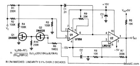
A range of 10 Hz to 10 kHz is covered by this circuit. (View)
View full Circuit Diagram | Comments | Reading(665)
AUTO_LIGHTS_ON_REMINDER
Published:2009/6/24 21:58:00 Author:May

The alarm is composed of a diode, buzzer, and limiting resistor. The diode serves as a switch which allows the buzzer to sound off only when the light switch is closed and the ignition is turned off. (View)
View full Circuit Diagram | Comments | Reading(590)
SEQUENTIAL_FLASHER_FOR_AUTOMOTIVE_TURN_SIGNALS
Published:2009/6/24 21:58:00 Author:May

When the turn signal switch 51 is closed, lamp #1 will be activated and capacitor C1 will charge to the triggered voltage of Q1. As soon as the anode voltage on Q1 exceeds its gate voltage by 0.5 V, Q1 will switch into the low resistance mode, thereby triggering SCR1 to activate lamp #2 and the second timing circuit.After Q2 switches into the low resistance state, SCR2 will be triggered to activate lamp #3. When the thermal flasher interrupts the current to all three lamps, SCR1 and SCR2 are commutated and the circuit is ready for another cycle. (View)
View full Circuit Diagram | Comments | Reading(1265)
VOLTAGE_CONTROLLED_AUDIO_AMPLIFIER
Published:2009/6/24 21:56:00 Author:May
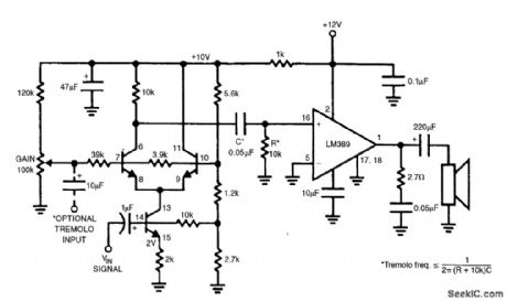
The LM389 has internal transistors used in this circuit. (View)
View full Circuit Diagram | Comments | Reading(1342)
OVERSPEED_INDICATOR
Published:2009/6/24 21:56:00 Author:May

An op-amp comparator is used to compare the converter output with a dc threshold vol-tage. The circuit flashes the LED when the input frequency exceeds 100 Hz. Increases in frequency raise the average current out of ter-minal 3 so that frequencies above 100 Hz re-duce the charge time of C2, increasing the LED flashing rate. IC = LM2907 or LM2917 (View)
View full Circuit Diagram | Comments | Reading(1266)
VOLTAGE_CONTROLLED_AMPLIFIER
Published:2009/6/24 21:55:00 Author:May
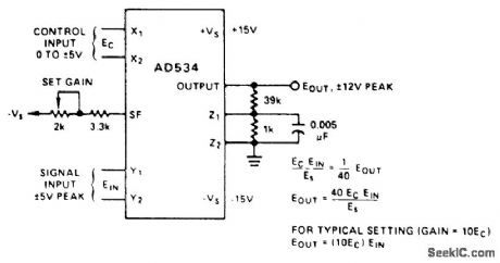
A constant or varying signal applied to the X input, Ec, controls the gain for a constant or vari-able signal applied to the Y input, Ein. The inputs could be interchanged.For this circuit, the set gain potentiometer is typically adjusted to provide a calibration for gain of Z 10 per-V-of-Ec. The bandwidth is dc to 30 kHz, independent of the gain. The wideband noise (10 Hz to 30 kHz) is 3 mV rms, typically, corresponding to full-scale signal-to-noise of 70 dB. Noise, referred to the signal input (Ec=±5V) is 60μV rms, typically. (View)
View full Circuit Diagram | Comments | Reading(0)
CAR_BATTERY_CONDITION_CHECKER
Published:2009/6/24 21:55:00 Author:May
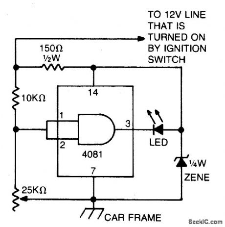
This circuit uses an LED and 4081 CMOS integrated circuit. The variable resistor sets the voltage at which the LED turns on. Set the control so that the LED lights when the voltage from the car's ignition switch drops below 13.8 volts. The LED normally will light every now and then for a short period of time. But, if it stays on for very long, your electrical system is in trouble. (View)
View full Circuit Diagram | Comments | Reading(1060)
WINDSHIELD_WASHER_FLUID_WATCHER
Published:2009/6/24 21:54:00 Author:May
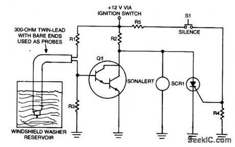
This circuit relies upon the minute current between two conductive probes sus-pended in a washer fluid reservoir. When the level is below the probes, Q1 turns on and the Sonolert sounds. (View)
View full Circuit Diagram | Comments | Reading(573)
HEADLIGHT_DELAY_UNIT
Published:2009/6/24 21:53:00 Author:May

This circuit will operate a car's headlights for a predetermined time to light up the drive-way or path after the driver has left the car. SQ1 is pushed and Q2 is turned on closing the relay and turning on the car's headlights. C1 begins to charge through VR1 until Q1 turns on, turning Q2 off. The relay will then open switching off both the lights and the unit. The delay is governed by the time taken for the capacitor to charge, which is about one minute. (View)
View full Circuit Diagram | Comments | Reading(1337)
VIDEO_LINE_DRIVER
Published:2009/6/24 21:53:00 Author:May
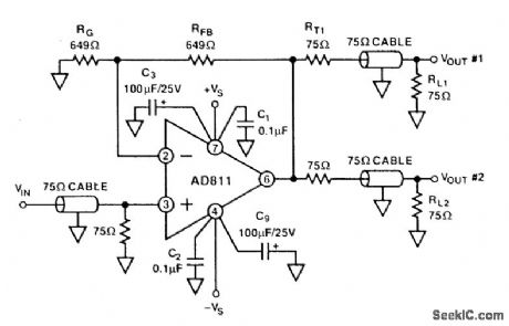
This video buffer/line driver operates at a gain of +2 and drives a pair of 75-Ω lines with 75-Ω back terminations. The overall terminated gain is unity. (View)
View full Circuit Diagram | Comments | Reading(745)
| Pages:1326/2234 At 2013211322132313241325132613271328132913301331133213331334133513361337133813391340Under 20 |
Circuit Categories
power supply circuit
Amplifier Circuit
Basic Circuit
LED and Light Circuit
Sensor Circuit
Signal Processing
Electrical Equipment Circuit
Control Circuit
Remote Control Circuit
A/D-D/A Converter Circuit
Audio Circuit
Measuring and Test Circuit
Communication Circuit
Computer-Related Circuit
555 Circuit
Automotive Circuit
Repairing Circuit