
Circuit Diagram
Index 1322
HIGH_IMPEDANCE_LOW_CAPACITANCE_WIDEBAND_BUFFER
Published:2009/6/24 22:46:00 Author:May
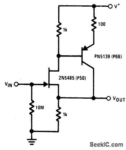
The 2N5485 has low input capacitance which makes this compound series-feedback buffer a wide-band unity gain amplifier. (View)
View full Circuit Diagram | Comments | Reading(803)
ADJUSTABLE_LIGHT_DETECTION_SWITCH
Published:2009/6/24 22:45:00 Author:May


R2 sets the circuit's threshold. When the light intensity at PCI's surface is decreased, the resistance of PC1 a cadmium-sulfide photoresistor is increased. This decreases the voltage atthe inverting input of the 741. When the reference voltage atthe 741's noninverting input isproperly adjusted via R2, the comparator will switch from low to high when PC1 is darkened. This turns on Q1 which, in turn, pulls in relay K1. (View)
View full Circuit Diagram | Comments | Reading(944)
OPTICAL_SCHMITT_TRIGGER
Published:2009/6/24 22:44:00 Author:May


This circuit shows a 555 with its trigger and threshold inputs connected together used to energize a relay when the light level on a photoconductive cell falls below a preset value. Circuit can be used in other applications where a high input impedance and low output impedance are required with the minimum component count. (View)
View full Circuit Diagram | Comments | Reading(994)
SINGLE_SUPPLY_AC_BUFFER_HIGH_SPEED
Published:2009/6/24 22:44:00 Author:May

View full Circuit Diagram | Comments | Reading(522)
SINGLE_SUPPLY_AC_BUFFER_AMPLIFIER
Published:2009/6/24 22:43:00 Author:May
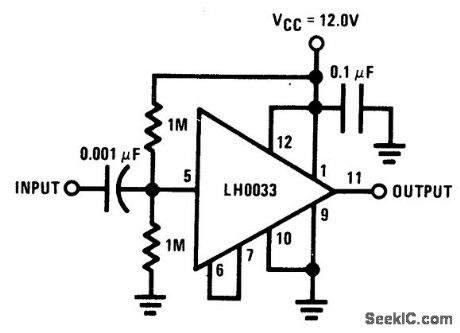
The input is dc biased to mid-operating point and is ac coupled. Its input impedance is approximately 500K at low frequencies. For dc loads referenced to ground, the quiescent cur-rent is increased by the load current set at the input dc bias voltage. (View)
View full Circuit Diagram | Comments | Reading(0)
TIME_DELAY_FLASH_TRIGGER_CIRCUIT
Published:2009/6/24 22:43:00 Author:May

The circuit is built around a single 4093 quad 2-input NAND Schmitt trigger. Two gates from that quad package (U1-a and U1-b) are configured as a set-reset flip-flop. (View)
View full Circuit Diagram | Comments | Reading(1455)
SINE_WAVE_OUTPUT_BUFFER_AMPLIFIER
Published:2009/6/24 22:42:00 Author:May
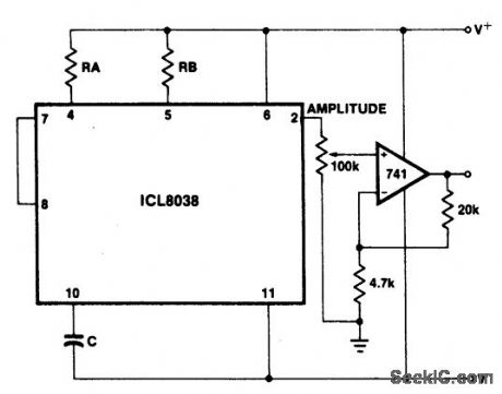
The sine wave output has a relatively high output impedance (1K typ). The circuit provides buffering, gain, and amplitude adjust ment. A simple op amp follower could also be used. (View)
View full Circuit Diagram | Comments | Reading(583)
PHOTODIODE_AMPLIFIER
Published:2009/6/24 22:42:00 Author:May
View full Circuit Diagram | Comments | Reading(2160)
RECEIVER_FOR_50_kHz_FM_OPTICAL_TRANSMITTER
Published:2009/6/24 22:40:00 Author:May

This circuit consists of a L14G2 detector, two stages of gain, and a FM demodulator. Better sensitivity can be obtained using more stages of stabilized gain with AGC. (View)
View full Circuit Diagram | Comments | Reading(0)
PHASE_SHIFTER_WITH_EIGHT_OUTPUTS
Published:2009/6/24 22:39:00 Author:May

The circuit consists of eight cascaded identical cells, each cell being a dc-controlled active phase shifter. Because the dc control is common for all shifters, the circuit is adjusted by trimming RA so that the phase difference between V01 and Vi is zero. As a result, each shifter will introduce a phase difference of exactly π/r. The eight signals for PSK are available at the op amps' outputs.
Phase accuracy is acceptable for 1%-tolerance resistors and 5%-tolerance 100-nF capacitors. Also, the amplitude of Vi (which is a 1700-Hz sine wave), should not exceed 1 V. (View)
View full Circuit Diagram | Comments | Reading(723)
AUTOMATIC_NIGHT_LIGHT
Published:2009/6/24 22:34:00 Author:May

During daylight hours, the L14B photo-Darlington (JEDEC registered as 2N5777 through 2N5780) shunts all gate current to ground. At night, the L14B effectively provides a high resistance, diverting the current into the gate of the C106B and turning on the lamp. (View)
View full Circuit Diagram | Comments | Reading(1541)
PHASE_SPLITTER_CIRCUIT
Published:2009/6/24 22:33:00 Author:May

This phase splitter uses a 2N2222 (or other general purpose npn transistor) to achieve outputs that are 180° out ofphase. (View)
View full Circuit Diagram | Comments | Reading(2464)
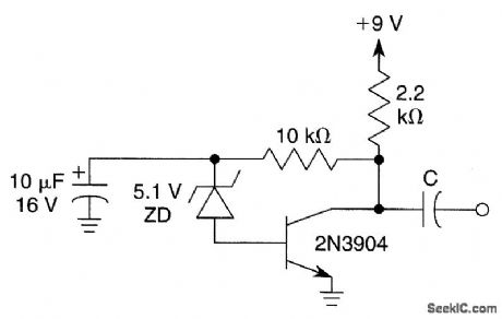
WHITE_NOISE_GENERATOR
Published:2009/6/24 22:33:00 Author:May

Here, a 2N3904 E-B junction is used as a noise generator, reversed bias. C is chosen to pass the lowest-desired frequency components of the noise. (View)
View full Circuit Diagram | Comments | Reading(2561)
ZENER_DIODE_WHITE_NOISE_GENERATOR
Published:2009/6/24 22:32:00 Author:May
This circuit uses a Zener diode as a noise source. C is chosen to pass the lowest-desired frequency components of the noise. (View)
View full Circuit Diagram | Comments | Reading(3573)
BATTERY_THRESHOLD_INDICATOR
Published:2009/6/24 22:32:00 Author:May

View full Circuit Diagram | Comments | Reading(570)
BATTERY_LEVEL_INDICATOR
Published:2009/6/24 22:32:00 Author:May

View full Circuit Diagram | Comments | Reading(107)
LONG_TAILED_PAIR_PHASE_SPLITTER
Published:2009/6/24 22:31:00 Author:May

The single-phase input produces out-of-phase outputs at the collectors of Q1 and Q2. (View)
View full Circuit Diagram | Comments | Reading(758)
PRECISION_PHOTODIODE_COMPARATOR_
Published:2009/6/24 22:31:00 Author:May

R1 sets the comparison level. At comparison, the photodiode has less than 5 mV across it, decreasing dark current by an order of magnitude. IC = LM 111/211/311. (View)
View full Circuit Diagram | Comments | Reading(728)
LOW_BATTERY_INDICATOR
Published:2009/6/24 22:31:00 Author:May

The indicator flashes an LED when the battery voltage drops below a certain threshold. 2N4274 emitter-base junction serves as a zener which establishes about 6V on the L161's positive input. As the battery drops, the L161 output goes high. This turns on the Darlington, which discharges C1 through the LED. The interval between flashes is roughly two seconds and gives a low battery warning with only 10 μA average power drain. (View)
View full Circuit Diagram | Comments | Reading(3252)
10_GHz_WAVEGUIDE_TRANSITION_FOR_AMATEUR_RADIO_USE
Published:2009/6/24 22:31:00 Author:May
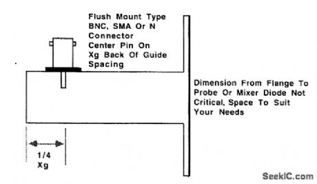
A transistor adapts the waveguide to coaxial cable or other types of transmission lines. (View)
View full Circuit Diagram | Comments | Reading(1038)
| Pages:1322/2234 At 2013211322132313241325132613271328132913301331133213331334133513361337133813391340Under 20 |
Circuit Categories
power supply circuit
Amplifier Circuit
Basic Circuit
LED and Light Circuit
Sensor Circuit
Signal Processing
Electrical Equipment Circuit
Control Circuit
Remote Control Circuit
A/D-D/A Converter Circuit
Audio Circuit
Measuring and Test Circuit
Communication Circuit
Computer-Related Circuit
555 Circuit
Automotive Circuit
Repairing Circuit