
Circuit Diagram
Index 1325
AUTOMOTIVE_CHARGER_FOR_NI_CAD_BATTERY_PACKS
Published:2009/6/24 22:16:00 Author:May

The number of silicon diodes across the output is determined by the voltage of the battery pack. Figure each diode at 0.7 volt. For example, a 10.9- volt pack would require 10.9/0.7 = 15.57, or 16 diodes. (View)
View full Circuit Diagram | Comments | Reading(562)
HIGH_IMPEDANCE_DIFFERENTIAL_AMPLIFIER
Published:2009/6/24 22:16:00 Author:May
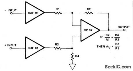
View full Circuit Diagram | Comments | Reading(0)
SIMPLE_OSCILLOSCOPE_TIMEBASE_GENERATOR
Published:2009/6/24 22:16:00 Author:May
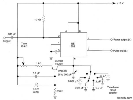
The 555 timer generates both a linear ramp and an output for Z-axis modulations of the CRT electron beam. (View)
View full Circuit Diagram | Comments | Reading(720)
LOW_DRAIN_METER_AMPLIFIER
Published:2009/6/24 22:16:00 Author:May
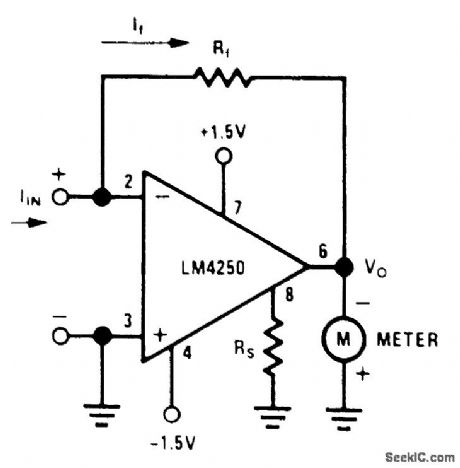
Meter amplifiers normally require one or two 9-V transistor batteries. Because of the heavy cur-rent drain on these supplies, the meters must be switched to the OFF position when not in use. The meter circuit described here operates on two 1.5-V flashlight batteries and has a quiescent power drain so low that no on/off switch is needed. A pair of Eveready No. 950 D cells will serve for a min-irnum of one year without replacement. As a dc ammeter, the circuit will provide current ranges as low as 100 nA full-scale.
The basic meter amplifier circuit shown is a current-to-voltage converter. Negative feedback around the amplifier ensures that currents IIN and If are always equal, and the high gain of the op amp ensures that the input voltage between pins 2 and 3 is in the microvolt region. Output voltageVO is therefore equal to -IfRf. Considering the ±1.5-V sources (±1.2 V end of life) a practical value ofVO for full-scale meter deflection is 300 mV. With the master bias-current setting resistor (RS) set at 10 MΩ, the total quiescent current drain of the circuit is 0.6μA for a total power supply drain of 1.8 pW. The irtput bias current, required by the amplifier at this low level of quiescent current, is in the range of 600μA. (View)
View full Circuit Diagram | Comments | Reading(681)
DIFFERENTIAL_INPUT_INSTRUMENTATION_AMPLIFIER_
Published:2009/6/24 22:15:00 Author:May

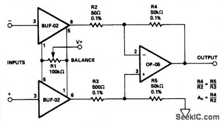
View full Circuit Diagram | Comments | Reading(599)
NI_CAD_CHARGER_WITH_CURRENT_AND_VOLTAGE_LIMITING
Published:2009/6/24 22:14:00 Author:May

Lamp L1 will glow brightly and the LED will be out when the battery is low and being charged, but the LED will be bright and the light bulb dim when the battery is almost ready. L1 should be a light bulb rated for the current you want (usually the battery capacity divided by 10).Diode Dl should be at least 1 A,and Z1is a 1 W zerLer diode with a voltage determinedby the full-charge battery voltage Π11nUS 1,5 V。After the battery IS fully charged, the circuit、vill float it at about battery capacity divided by100 mA. (View)
View full Circuit Diagram | Comments | Reading(571)
SIMPLE_SPECTRUM_ANALYZER_ADAPTOR_FOR_SCOPES
Published:2009/6/24 22:14:00 Author:May

Suitable for monitoring an amateur band or a segment of the radio spectrurn, this simple adaptor uses an NE602 mixer-oscillator chip to produce a 455-kHz IF signal, which U2 amplifies, then feeds to detector D2 and the Y axis of an oscilloscope. VT is used to drive the horizontal axis input of a scope. L2 and L3 are coils suitable for the frequency range in use. For this circuit, coils are shown for the 10- to 15-MHz range. L2 and L3 are wound on Amidon Associates, T-37 or T-50 toroidal cores, and L1 is a commercial or homemade variable inductor, etc. (View)
View full Circuit Diagram | Comments | Reading(1603)
200_mA_HOUR,12_V_NI_CAD_BATTERY_CHARGER
Published:2009/6/24 22:13:00 Author:May

This circuit charges the battery at 75 mA until the battery is charged, then it reduces the current to a trickle rate. It will completely recharge a dead battery in four hours and the battery can be left in the charger indefinitely. To set the shut-off point, connect a 270-ohm, 2-watt resistor across the charge terminals and adjust the pot for 15.5 volts across the resistor. (View)
View full Circuit Diagram | Comments | Reading(1228)
3INSTRUMENTATION_AMPLIFIER
Published:2009/6/24 22:13:00 Author:May
View full Circuit Diagram | Comments | Reading(691)
AUDIBLE_VOLTAGE_INDICATOR
Published:2009/6/24 22:13:00 Author:May

The audible voltmeter can be used to test for ac or dc voltages in a circuit. With S1 closed, the circuit can be used to test for voltages between 4 and 24 V, and when S1 is open, it can be used to check for the presence voltages of up to 200 V. (View)
View full Circuit Diagram | Comments | Reading(667)
DOUBLE_ENDED_VOLTAGE_MONITOR
Published:2009/6/24 22:12:00 Author:May
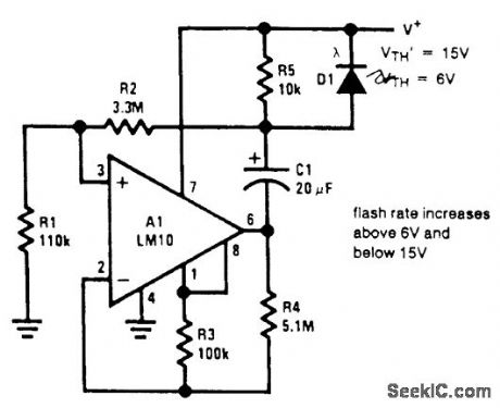
This circuit has the added feature that it can sense an over-voltage condition. The lower activa-Lion threshold is given by equation (1), but above a threshold, oscillation again ceases. Below VTH, the op amp output is saturated negative, but above VTH, it is saturated positive. The flash rate approaches zero near either limit. (View)
View full Circuit Diagram | Comments | Reading(0)
INSTRUMENTATION_AMPLIFIER(TWO_OP_AMP_DESIGN)
Published:2009/6/24 22:12:00 Author:May
View full Circuit Diagram | Comments | Reading(571)
AUTOMATIC_SHUTOFF_BATTERY_CHARGER
Published:2009/6/24 22:11:00 Author:May

Adjust by setting the 500 ohm resistor while attached to a fully charged battery. (View)
View full Circuit Diagram | Comments | Reading(1207)
BATTERY_CHARGER
Published:2009/6/24 22:11:00 Author:May

A diac is used in the gate circuit to provide a threshold level for firing the triac. C3 and R4 provide a transient suppression network. RI, R2, R3, C1, and C2 provide a phase-shift network for the signal being applied to the gate. R1 is selected to limit the maximum charging cur-rent at full rotation of R2. (View)
View full Circuit Diagram | Comments | Reading(0)
INEXPENSIVE_VOLTAGE_CALIBRATOR
Published:2009/6/24 22:10:00 Author:May
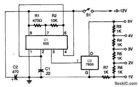
In the voltage calibrator, two low-cost ICs-a 555 oscillator/timer and a 78055 5-V 1.5-A voltage regulator-along with a precision voltage divider network are used to provide outputs of 1- to 5-V peak-to-peak. (View)
View full Circuit Diagram | Comments | Reading(1394)
SIMPLE_3_DIGIT_DVM
Published:2009/6/24 22:10:00 Author:May

A CA3162ZE A-D converter drives a CA3161 BCD decoder/driver and LED display to form a sim-ple DVM circuit. The 50-kΩ gain control and 100-kΩ/10-kΩ voltage divider determine full-scale range. (View)
View full Circuit Diagram | Comments | Reading(1832)
EXPANDED_SCALE_dc_METER_FOR_12_V_SYSTEMS
Published:2009/6/24 22:08:00 Author:May
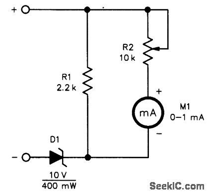


This circuit can be used to monitor a 12-V system with a meter reading10 V to another volt-age. Expect 10 to 20 V, depending on the setting of R2. Depending on the characteristics of D1, R1 might be increased or eliminated entirely. (View)
View full Circuit Diagram | Comments | Reading(567)
HIGH_IMPEDANCE_BRIDGE_AMPLIFIER
Published:2009/6/24 22:08:00 Author:May
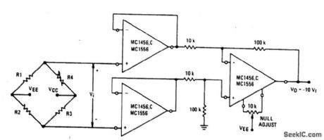
View full Circuit Diagram | Comments | Reading(588)
dc_VOLTMETER
Published:2009/6/24 22:08:00 Author:May
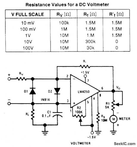
A wide-range voltmeter circuit. This inverting amplifier has a gain varying from -30 for the 10-mV full-scale range to -0.003 for the 100-V full-scale range. Diodes D1 and D2 provide com-plete amplifier protection for input overvoltages as high as 500V on the 10-mV range, but if over-voltages of this magnitude are expected under continuous operation, the power rating of RV should be adjusted accordingly (View)
View full Circuit Diagram | Comments | Reading(2564)
HIGH_GAIN_DIFFERENTIAL_INSTRUMENTATION_AMPLIFIER
Published:2009/6/24 22:07:00 Author:May
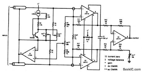
This circuit includes input guarding, cable bootstrapping, and bias current compensation. Differential bandwidth is reduced by C1 which also makes common-mode rejection less dependent on matching of input amplifiers. (View)
View full Circuit Diagram | Comments | Reading(575)
| Pages:1325/2234 At 2013211322132313241325132613271328132913301331133213331334133513361337133813391340Under 20 |
Circuit Categories
power supply circuit
Amplifier Circuit
Basic Circuit
LED and Light Circuit
Sensor Circuit
Signal Processing
Electrical Equipment Circuit
Control Circuit
Remote Control Circuit
A/D-D/A Converter Circuit
Audio Circuit
Measuring and Test Circuit
Communication Circuit
Computer-Related Circuit
555 Circuit
Automotive Circuit
Repairing Circuit