
Circuit Diagram
Index 1329
SIMPLE_ULTRASONIC_GENERATOR
Published:2009/6/24 21:35:00 Author:May
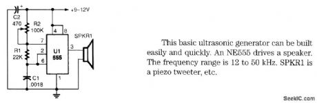
This basic ultrasonic generator can be built easily and quickly. An NE555 drives a speaker.The frequency range is 12 to 50 kHz. SPKRI is a piezo tweeter, etc. (View)
View full Circuit Diagram | Comments | Reading(2141)
ULTRASONIC_PROXIMITY_SENSOR
Published:2009/6/24 21:34:00 Author:May
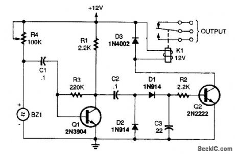
A 100-kΩ potentiometer, R4, sets the cur-rent fed to the Sonalert sounder. The poten-tiometer is adjusted to a point where the sounder just begins to make an audible sound. A single-transistor audio amplifier (Q1) is coupled to the positive side of the sounder and its output is fed to a voltage-doubler circuit. The doubler's dc out-put drives the base of Q2, which, in turn, oper-ates the relay (K1). As long as the Sonalert is producing a sound, the relay stays energized.When a solid object is moved in close prox-imity to the front of the sounder, the Q of the piezo element is lowered and the Sonalert's inter-nal circuit ceases to operate; as a result, the relay drops out. By carefully adjusting R4, the circuit can be made quite sensitive. (View)
View full Circuit Diagram | Comments | Reading(1786)
ULTRASONIC_cw_TRANSCEIVER
Published:2009/6/24 21:33:00 Author:May

With the telegraph key at S2 up (open), the 567 PLL's input at pin 3 is coupled to the output of Q3. Transistors Q3 and Q4 are operat-ing in a high-gain, two-stage audio-amplifier circuit. The piezo speaker is coupled to the in-put of the amplifier though a 0.1-μF capacitor and a 680-Ω isolation resistor.In the receive mode, the piezo speaker oper-ates as a sensitive microphone. Ultrasonic signals travel from the microphone through the two-stage amplifier to the input of the 567, and, if the signal's frequency is within the IC's bandwidth, the LED will light and piezo-sounder BZ1 will sing out foreach dit and dah received. The receiver can be tuned to the incoming ultrasonic signal by adjust-ing R17. Of course, adjusting that potentiometer also changes the transmitter's frequency.The transmitter operates each time the S2 is closed. When the key is closed, diode D3 supplies a path to ground for BZ1, causing that sounder to produce an audible signal for each dit and dah transmitted. Also, Q2's bias is taken to ground through D2, allowing Q1 to pass the 567's square-wave signal on to the input of the power amplifier and out through the speaker. (View)
View full Circuit Diagram | Comments | Reading(0)
FREQUENCY_SWITCHER
Published:2009/6/24 21:32:00 Author:May

This transistor can achieve frequency switching in this CMOS astable oscillator. (View)
View full Circuit Diagram | Comments | Reading(0)
COMPACT_IR_RECEIVER
Published:2009/6/24 21:32:00 Author:May
View full Circuit Diagram | Comments | Reading(0)
ULTRASONIC_MOTION_DETECTOR
Published:2009/6/24 21:32:00 Author:May

A 567 PLL IC operates in a dual-function mode as a signal generator and an FM receiver. The 567's square-wave output at pin 5 is coupled to the base of Q1, and from Q1's emitter to the input of the power amplifier (Q2 and Q6). The output drives the piezo speaker, SPKR1.
The receive portion of the circuit operates as follows: transistors Q3 and Q4 are connected in a two-stage, high-gain, audio-frequency amplifier circuit, with the input connected to a second piezo speaker (SPKR2) operating as a sensitive microphone. The amplifier's output is coupled to the 567's input at pin 3. When an in-band signal is received, the LED lights.
The 567's FM output is coupled from pin 2 to the input of a very-low-frequency single-transistor amplifier, Q5. The amplifier's output at Q5's collector drives a voltage-doubler circuit (C11, D1, D2, and C12). The dc output feeds a 0- to 1-mA analog meter.
By placing the two pigzo speakers one foot apart and aiming them in the same direction, toward a nonmoving solid object, the signal from the transmitter's speaker urill reflect back into the receiver's speaker, and the frequency at the 567's input will be the same as the one being transmitted.
The ac output at pin 2 is zero when the outgoing and incoming frequencies are the same. How-ever, when the signal is reflected from a moving object, the received frequency will be either lower or higher than the transmitted one. If the object is moving away from the speakers, the received fre-quency will be lower; if the object is moving toward the speakers, the frequency will be higher.
The pin-2 signal is fed through a 470-pF capacitor to the base of Q5, where the signal is ampli-fied and fed to a voltage doubler, and then on to a meter circuit.
If you wish, the voltage doubter and meter can be removed and replaced with headphones connected between the negative side of C11 and circuit ground. That will allow you to listen to the difference-frequency signal as objects move in front of the speakers. (View)
View full Circuit Diagram | Comments | Reading(0)
CMOS_VFO
Published:2009/6/24 21:31:00 Author:May

The circuit shown has a frequency range of 2 Hz to 30 kHz. R2 is a linear or log potentiometer. (View)
View full Circuit Diagram | Comments | Reading(0)
IR_REMOTE_CONTROL_TRANSMITTER/RECEIVER
Published:2009/6/24 21:30:00 Author:May
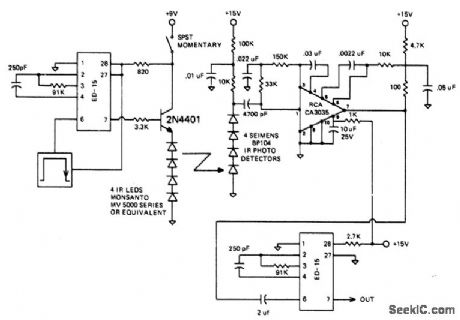
The circuit is designed to operate at 25 kHz. The data stream turns the 2N4401 hard on or off depending upon the coded state. This in turn switches the series infrared LEDs on and off. The receiver circuit consists of a three stage amplifier with photo diodes arrayed for maximum coverage of the reception area. The range of this set-up should be about 10 meters. (View)
View full Circuit Diagram | Comments | Reading(0)
IR_TYPE_DATA_LINK
Published:2009/6/24 21:29:00 Author:May

View full Circuit Diagram | Comments | Reading(0)
CRYSTAL_OSCILLATOR
Published:2009/6/24 21:28:00 Author:May

Circuit NotesStable VXO using 6-or 8-MHz crystals uses a capacitor and an inductor to achieve frequency pulling on either side of series resonance. (View)
View full Circuit Diagram | Comments | Reading(0)
ULTRASONIC_REMOTE_CONTROL_TESTER
Published:2009/6/24 21:27:00 Author:May
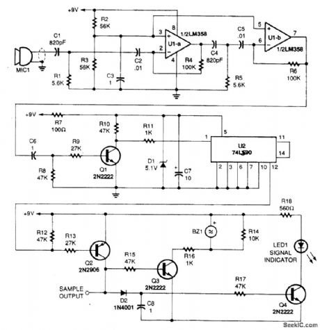
This circuit picks up the ultrasonic tone via MIC1, amplifies it, and divides it by 10 in IC U2, a 74LS90. The output of U2 drives an audio amplifier and a piezoelectric element is used as a speaker. (View)
View full Circuit Diagram | Comments | Reading(0)
VISUAL_ZERO_BEAT_INDICATOR
Published:2009/6/24 21:27:00 Author:May

Light-emitting diodes connected with re-verse polarity provide a visual indication of zero-beat ffequency. Each LED is on for only half a cycle of the input. When the input fre-quency is more than 1 kilohertz away from the zero-beat frequency, both LEDs appear to be on all the time. As the input frequency comes within about 20 hertz of zero beat, the LEDs will flicker until zero beat is reached. Both LEDs glow or flicker until zero beat is reached, when they go out. (View)
View full Circuit Diagram | Comments | Reading(1325)
SIMPLE_NTSC_GRAY_SCALE_VIDEO_GENERATOR
Published:2009/6/24 21:46:00 Author:Jessie

A 4.032-MHz crystal oscillator (256 x horizontal line scan rate) drives a BCD counter. The binary outputs of the counter are fed to R2 through R5, a simple weighting network for D/A conversion, re-sulting in a staircase video output with a rep rate of 15.75 kHz. This circuit should be useful for am-ateur TV linearity testing and setup purposes. (View)
View full Circuit Diagram | Comments | Reading(0)
ADJUSTABLE_VFO_TEMPERATURE_COMPENSATOR
Published:2009/6/24 21:45:00 Author:Jessie

Use of a differential capacitor allows temperature compensation of LC circuit using an NPO and N1500 ceramic. C6 is a differential capacitor that has two stators and one common rotor. When one capacitance (stator) is maximum, the other is minimum. L1, C1, C2, and C3 are tuning, trimming, and fixed capacitors, respectively. (View)
View full Circuit Diagram | Comments | Reading(1129)
DIFFERENTIAL_INPUT_INSTRUMENTATION_AMPLIFIER_WITH_HIGH_COMMON_MODE_REJECTION
Published:2009/6/24 21:45:00 Author:Jessie
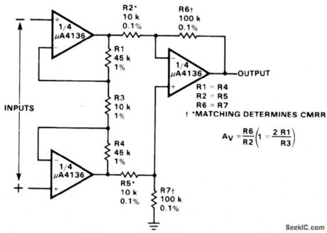
View full Circuit Diagram | Comments | Reading(677)
VIDEO_CABLE_DRIVER
Published:2009/6/24 21:45:00 Author:Jessie

This is a MAX436 coaxial-cable driving circuit (View)
View full Circuit Diagram | Comments | Reading(1174)
VIDEO_IF_AMPLIFIER_DETECTOR
Published:2009/6/24 21:44:00 Author:Jessie

View full Circuit Diagram | Comments | Reading(972)
NTSC_TO_RGB_CONVERTER
Published:2009/6/24 21:43:00 Author:Jessie

This circuit takes baseband NTSC video, decodes it, and derives RGB video suitable for driving a color multisync computer monitor. This enables the user to take advantage of the generally better resolution of computer monitors. (View)
View full Circuit Diagram | Comments | Reading(4920)
TRIPLE_OP_AMP_INSTRUMENTATION_AMPLIFIER
Published:2009/6/24 21:43:00 Author:Jessie
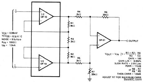
View full Circuit Diagram | Comments | Reading(616)
ZERO_CENTER_INDICATOR_FOR_FM_RECEIVERS
Published:2009/6/24 21:26:00 Author:May

To adjust, tune in a station and adjust the 1 M pot for a null. Then ask the station to modulate and fine adjust so modulation peaks don't light the LEDs. Stations are properly tuned when neither LED is lit. (View)
View full Circuit Diagram | Comments | Reading(0)
| Pages:1329/2234 At 2013211322132313241325132613271328132913301331133213331334133513361337133813391340Under 20 |
Circuit Categories
power supply circuit
Amplifier Circuit
Basic Circuit
LED and Light Circuit
Sensor Circuit
Signal Processing
Electrical Equipment Circuit
Control Circuit
Remote Control Circuit
A/D-D/A Converter Circuit
Audio Circuit
Measuring and Test Circuit
Communication Circuit
Computer-Related Circuit
555 Circuit
Automotive Circuit
Repairing Circuit