
Signal Processing
Index 171
555 color photo printing & washing instrument circuit
Published:2011/5/20 8:05:00 Author:TaoXi | Keyword: color photo, printing, washing, instrument
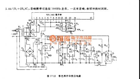
As the figure shown, the printing & washing instrument is composed of the temperatrure controller, the washing timer and the timing buzzer.etc. The temperature control range is below 50℃, also it is free to adjust; the temperature control accuracy is +/-0.5℃; the timing time is 2 minutes 45 seconds +/- 1 sec; the heating time is 1 hour.
The washing timing buzzer is composed of the IC2 and IC3, there is no need to adjust the time before using. The start timing circuit is composed of the IC2(555) and R5, RP2, C1, the timing time is td=1.1(R5+RP2)C1.
(View)
View full Circuit Diagram | Comments | Reading(449)
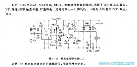
555 darkroom timer circuit (2)
Published:2011/5/24 2:50:00 Author:TaoXi | Keyword: darkroom, timer
Related components PDF download:
NE5553DG12
As the figure 17-15 shows, as the figure 17-15 shows, the monostable delay circuit is composed of the IC(555) and R2, RP1, C3.etc, when you press AN, 555 sets, VT1 conductd, the SRC trigger the conduction, and the lamp bulb gets the power. The timing time td=1.1RP1C3. When the time is up, 555 resets, VT1 cuts off, the light turns off.
If we changes the RP1 into the select switch with timing resistance, we can get the accurate timing.
(View)
View full Circuit Diagram | Comments | Reading(823)
TA1222N--the single chip integrated circuit of video small signal process
Published:2011/6/10 0:19:00 Author:qqtang | Keyword: single chip, integrated circuit, small signal
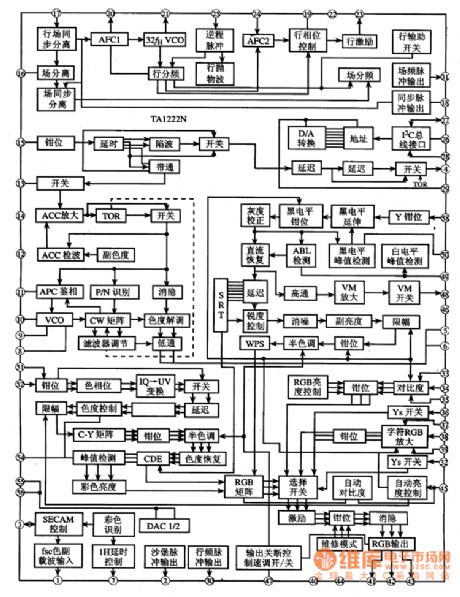
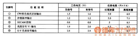
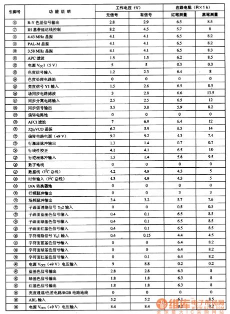
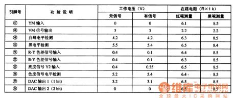
1.function featuresTA1222N is mainly used to fulfill functions of brightness signal process, chroma signal process and scanning deflection system small signal process, etc, the brightness signal process circuit includes high-quality image compensatory circuits, such as black LEV expanding circuit, DC LEV regain circuit, high brightness color circuit, delaying hole adjusting circuit and scanning speed signal generating circuit.2.pin functions and dataTA1222N is in 56-pin dual in-line package, whose pin functions are listed in Table 1.
(View)
View full Circuit Diagram | Comments | Reading(748)
TA7358P, TA7358AP and TA7358F--the integrated circuit of modulate high frequency
Published:2011/6/9 23:54:00 Author:qqtang | Keyword: integrated circuit, modulate high frequency
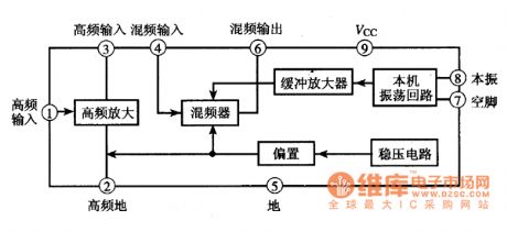
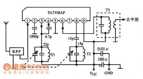
TA7358P/AP/F is the integrated circuit of modulate high frequency produced by Toshiba, which is widely used in all kinds of stereo radios, such as domestic stereo, car stereo and so on.1.function featuresTA7358P/AP/F contains FM high frequency amplifier, mixer, local oscillating circuit, bias and voltage steady circuit and buffer amplifier circuit, etc.The internal circuit of TA7358P/AP/F is shown in figure 1.Figure 1. The internal circuit of TA7358P/AP/F
2.pin functions and dataTA7358P/AP/F is in three types of packages, we are using different suffixes to represent them.
(View)
View full Circuit Diagram | Comments | Reading(7720)
Home Appliance Timing Blackouts Controller Circuit Composed of 555
Published:2011/6/2 3:35:00 Author:Joyce | Keyword: Home Appliance, Timing , Blackouts , Controller, 555
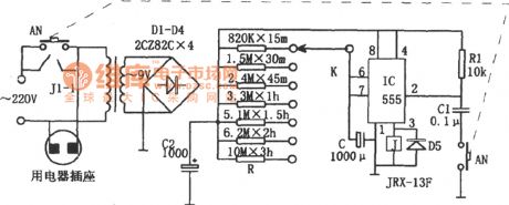
As shown in the figure is an electrical appliances timing blackouts control circuit.it consists of a step-down rectifier circuit, a timing circuit, and a relay control circuit etc among which the step-down rectifier circuit supplys power to the controller.
The timing circuit is a monostable delay circuit composed of IC (555) , R, C and some other components, and the timing time depends on the magnitude of charging and discharging time RC. When one stwiches on AN, 555 will start to set because the potential of feet ② is low level,and the high level output by feet③ will actuate relay J , so contacts J1-1 will be on to put the power through. At this time, timing starts and capacitor C will be charged through R. When the voltage of C is big enough to make the potential of feet⑥ of 555 higher than 2/3VDD, 555 will be reset,the low level output by feet③ will release relay J.so contacts J1-1 will cut off leading to appliance blackouts.The time for home appliance outages time can regulated by using K to choose different gears . (View)
View full Circuit Diagram | Comments | Reading(441)
First-order Active Phase Shift Oscillator Circuit
Published:2011/5/25 4:40:00 Author:Joyce | Keyword: First-order , Active , Phase Shift , Oscillator
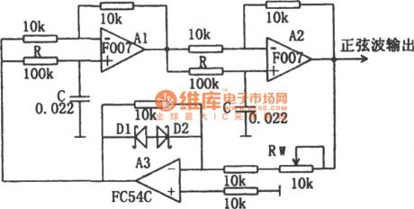
As shown in the figure is the first-order active phase shift oscillator circuit. In this circuit, the first-order active phase shift oscillator is composed of A1 and A2, which forms a loop circuit with A3.A3 is an inverse proportion amplifier, mainly responsible for amplification. The gain control of A3 is -1,and the shift phase is π.D1、D2 are voltage-regulator tubes 2DW7C which will help to stabilize the amplitude. In orderto meet the condition of oscillation, the absolute value of transmission coefficient βof the first-order active phase shift oscillator is 1. When the overall shift phase reaches π,the circuit would start oscillation. The oscillation frequency is:
f0=1/2πRC. (View)
View full Circuit Diagram | Comments | Reading(741)
2~20MHz Variable Frequency Transistor Oscillator Circuit
Published:2011/5/29 1:41:00 Author:Joyce | Keyword: 2~20MHz, Variable Frequency , Transistor Oscillator
View full Circuit Diagram | Comments | Reading(673)
OCL drived by NPN tube circuit
Published:2011/6/8 20:07:00 Author:chopper | Keyword: OCL, NPN

View full Circuit Diagram | Comments | Reading(581)
The electric adjuster circuit of temperature control fans
Published:2011/6/4 2:38:00 Author:qqtang | Keyword: electric adjuster, temperature control
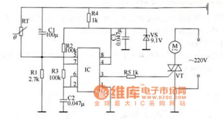
The working principle of the circuit This adjuster circuit consists of voltage-steady circuit, multi-resonate oscillator and control executing circuit, see as Figure 1.
In the circuit, the voltage-steady circuit consists of resistor R4, filtering capacitor C3 and voltage-steady diode VS; the oscillator consists of time-based integrated circuit IC, resistor R1-R3, capacitor C1 and C2 and thermistor RT; the control executing circuit consists of resistor R5, thyristor VT and fan motor M. When the power is on, the multi-oscillator is starting to work. (View)
View full Circuit Diagram | Comments | Reading(468)
Electronic Pain Relieving Instrument (the 2nd)
Published:2011/6/6 8:14:00 Author:Felicity | Keyword: Electronic Pain Relieving Instrument (the 2nd)
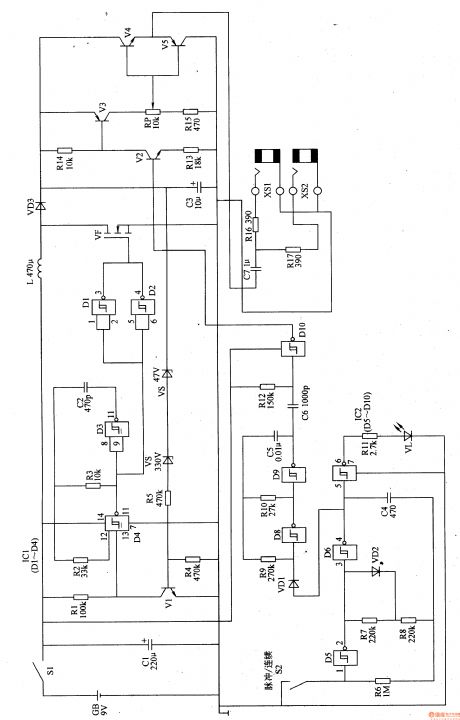
Work of the circuit
The circuit consists of high voltage making circuit, pulse making circuit and outputting circuit. (It is showed in picture 9-32.)
When S2 is turned on, the Electronic Pain Relieving Instrument works continuously. The 2Hz OSC does not work at all. The OSC outputs pulse continuously. And its working rate is about 10Hz. When you turn off S2 the Electronic Pain Relieving Instrument works intermittently. The OSC outputs pulse intermittently. Its working rate changes between 50Hz and 270Hz.
The pulse signal is amplified by V2-V5. The 2 poles on the outer side have pulse currency of low frequency. The pulse currency of low frequency stimulates the subcutaneous nurse and relieves pain. (View)
View full Circuit Diagram | Comments | Reading(609)
Electronic Pain Relieving Instrument (the 3rd)
Published:2011/6/6 8:15:00 Author:Felicity | Keyword: Electronic Pain Relieving Instrument (the 3rd)
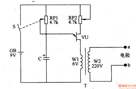
Work of the circuit
The circuit consists of potentiometer RG1 RG2, capacitor C, power switch S and pole A B. (It is showed in picture 9-33.)
Turn on switch S and the OSC starts working. The high voltage pulse is produced on the two ends of W2. The high voltage pulse is put on the pain area of the body by the poles. It can relieve the pain by stimulating the relevant acupoint or pain area.
Change the value of RG1 to change the frequency of OSC.
Change the value of RG2 to change the pulse voltage.
(View)
View full Circuit Diagram | Comments | Reading(810)
Electronic Massager (the 1st)
Published:2011/6/6 8:17:00 Author:Felicity | Keyword: Electronic Massager (the 1st)
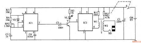
Work of the circuit
The circuit consists of low frequency OSC and electronic outputting circuit. (It is showed in picture 9-34.)
Turn on the switch S and low frequency OSC starts working. IC1’s pin 3 outputs pulse signal. The signal controls the working condition of V andIC2. When the pulse signal is right V works. When the pulse signal is negative V does not work. And VL does not shine. W2 produces pulse currency of low frequency. The pulse currency of low frequency stimulates the relevant acupoint or pain area to massage.
(View)
View full Circuit Diagram | Comments | Reading(1613)
four-divider frequency circuit
Published:2011/6/5 2:52:00 Author:John | Keyword: four-divider frequency
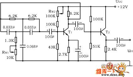
Figure: four-divider frequency circuit
Double T network RC sinusoidal oscillator circuit is shown in Figure 12-5. Disconnect the dual-T network to adjust the quiescent point of T1 pipe. And the UC1 is 6 ~ 7V. Access dual-T network and use the oscilloscope to observe the output waveform. If it does not start-up, adjust RW1 to start-up the circuit. Measure the oscillation frequency of the circuit and compare it with the calculated value. (View)
View full Circuit Diagram | Comments | Reading(544)
Hex counter circuit
Published:2011/6/5 3:16:00 Author:John | Keyword: Hex counter
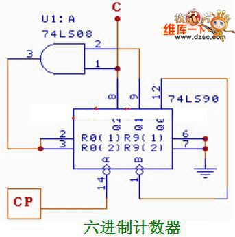
The number of two or more required to connect with cascaded 74LS90 chip. When the low chip reaches the full count, the highest point of the low chip low would be regarded as binary. And such would be sent to the CP end of a high chip.
Figure: Hex counter circuit (View)
View full Circuit Diagram | Comments | Reading(998)
32768Hz crystal oscillator circuit
Published:2011/6/4 9:35:00 Author:John | Keyword: crystal oscillator
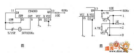
It consists of an integrated circuit CD4060, a crystal with resonant frequency of 30720Hz and other components. CD4060 is a 14-bit binary serial counter, divider and oscillator.
This circuit uses an external 30720Hz crystal to form a crystal oscillator. The oscillation signal is frequency processed through the inner parts of CD4060 and is to output accurate 60Hz frequency signal at the end of Q9 (30720 ÷ 29 = 60Hz). When the circuit is equipped with the double negative digital clock, 2b circuit shown in figure 2 can be used for polarity transform. VT1 and VT2 both use NPN type transistor, such as 9013 and 8050 and so on. Terminal A in the figure is equipped with positive power supply and Terminal B is equipped with negative power supply.
(View)
View full Circuit Diagram | Comments | Reading(2485)
8 binary counter circuit
Published:2011/6/5 3:23:00 Author:John | Keyword: 8 binary counter
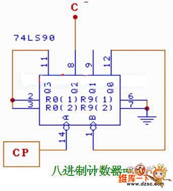
The number of two or more required to connect with cascaded 74LS90 chip. When the low chip reaches the full count, the highest point of the low chip low would be regarded as binary. And such would be sent to the CP end of a high chip. (View)
View full Circuit Diagram | Comments | Reading(459)
Four-frequency circuit
Published:2011/6/5 0:13:00 Author:John | Keyword: Four-frequency
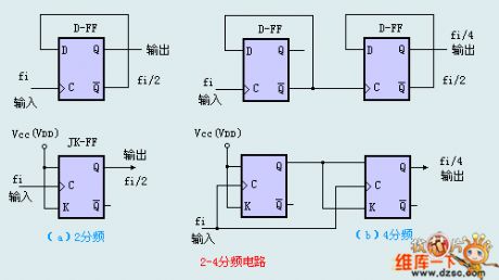
The figure is for N = two-quarter frequency ratio circuit. The circuit is often formed by double-D-FF or two JK-FF devices. Frequency division ratio of n> 4 circuit is often achieved by counter (for example a preset counter), which is generally without the need to combine a single FF.
The output duty cycle of the following divider circuit is 50%. It can be formed by D-FF or JK-FF. The JK-FF divider circuit tends to achieve a parallel and synchronous work easily. So such circuits can be suitable for high frequency applications. If the pin R, S (P) and other pins in FF are not used, it is necessary to connect to non-effective power or ground line according to the its functional requirements. (View)
View full Circuit Diagram | Comments | Reading(470)
RC series-parallel frequency selection network oscillator circuit
Published:2011/6/4 23:39:00 Author:John | Keyword: frequency selection network

Disconnect the RC series-parallel network to measure amplifier’s quiescent point and its voltage gain.
Disconnect the RC series-parallel network and the amplifier. Apply the sinusoidal signal of the function signal generator into the RC series-parallel network. Keep the signal amplitude still (about 3V). The frequency changes from low to high, so the output amplitude of RC series-parallel network would change. When the signal source reaches a certain frequency, the output of RC series-parallel network will reach the maximum value (about 1V). And when the input and output are with the phase, the signal source frequency is .
(View)
View full Circuit Diagram | Comments | Reading(696)
63 nary counter formed by cascade preset number circuit
Published:2011/6/5 5:16:00 Author:John | Keyword: 63 nary counter
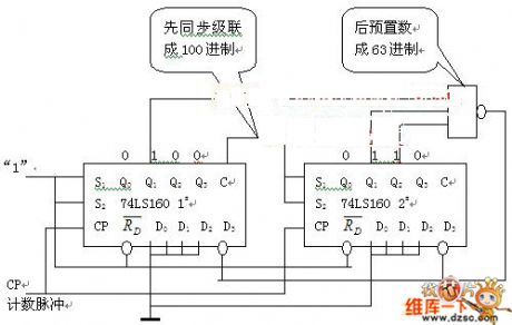
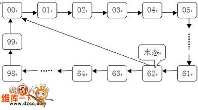
63 nary counter formed by cascade preset number circuit: We can also form 10i counter or 16i counter by the cascade method and use the preset method to constitute an arbitrary nary counter. 63 nary counter can be formed by 100 nary counter composed of two 10 nary counters (74LS160) and then can achieve the function by preset method. Its counting state transition is shown in Figure 2. It should be noted that 74LS160 has a synchronous preset number features and has no transition state.
Figure 2 63 nary counter formed by cascade preset number transition circuit (View)
View full Circuit Diagram | Comments | Reading(685)
63-nary counter circuit
Published:2011/6/5 8:35:00 Author:John | Keyword: 63-nary counter
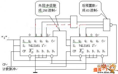
Figure:
View full Circuit Diagram | Comments | Reading(422)
| Pages:171/195 At 20161162163164165166167168169170171172173174175176177178179180Under 20 |
Circuit Categories
power supply circuit
Amplifier Circuit
Basic Circuit
LED and Light Circuit
Sensor Circuit
Signal Processing
Electrical Equipment Circuit
Control Circuit
Remote Control Circuit
A/D-D/A Converter Circuit
Audio Circuit
Measuring and Test Circuit
Communication Circuit
Computer-Related Circuit
555 Circuit
Automotive Circuit
Repairing Circuit