
Signal Processing
Index 162
The 4-time frequency multiply circuit (555)
Published:2011/6/17 6:57:00 Author:Borg | Keyword: frequency, multiply circuit
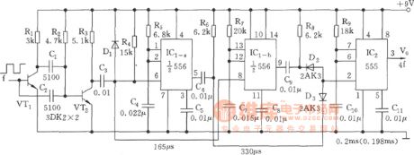
View full Circuit Diagram | Comments | Reading(541)
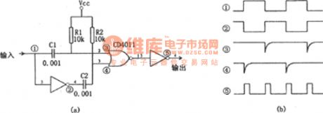
The 555 single stable circuit as the frequency splitter
Published:2011/6/17 6:52:00 Author:Borg | Keyword: single stable circuit, frequency splitter
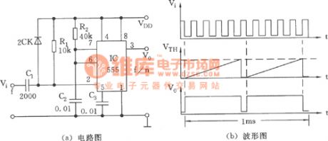
(a) circuit (b) waveform diagram (View)
View full Circuit Diagram | Comments | Reading(567)
The frequency synthesizer composed of CD4069, CD4013 and so on
Published:2011/6/17 6:49:00 Author:Borg | Keyword: frequency synthesizer
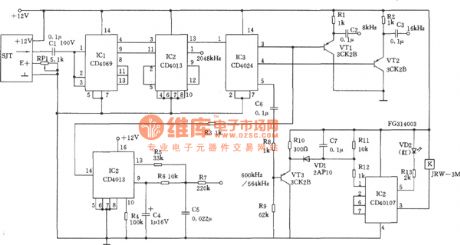
View full Circuit Diagram | Comments | Reading(745)
The M50117F/AP/BP/CP oscillating connection circuit
Published:2011/6/18 2:53:00 Author:Seven | Keyword: oscillating, connection circuit
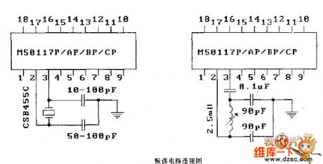
The oscillating connection circuit (View)
View full Circuit Diagram | Comments | Reading(451)
The MC9482 (electronic toy) remote reception decoding logic frame circuit
Published:2011/6/19 0:29:00 Author:Seven | Keyword: remote reception, logic frame
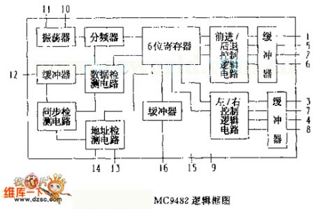
The MC9482 logic frame diagram (View)
View full Circuit Diagram | Comments | Reading(418)
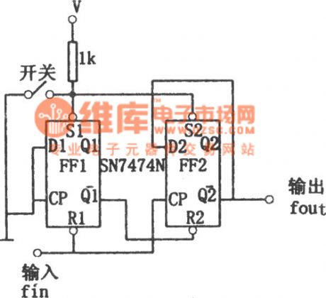
The simple frequency splitter circuit composed of SN7474N
Published:2011/6/17 22:19:00 Author:Borg | Keyword: frequency splitter
View full Circuit Diagram | Comments | Reading(1019)
The adjustable constant frequency splitter composed of S8424
Published:2011/6/17 21:59:00 Author:Borg | Keyword: adjustable constant, frequency splitter
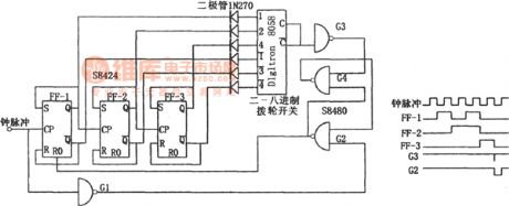
In the figure is the adjustable constant frequency splitter composed of S8424. This circuit consists of R-S trigger, gate circuit and binary-octal dial switch, which can do 1~8 frequency splitting. In the figure, 8058 is the switch, S8424 is the two-team RST trigger. S8480 is the 4*2 inputting NAND. The binary-octal dial switch is used to confirm the constant of the splitter, which makes sure the trigger is reset. If the binary-decimal dial switch is used, then an external trigger and two diodes are needed. (View)
View full Circuit Diagram | Comments | Reading(510)
The simple pulse frequency doubler
Published:2011/6/17 9:11:00 Author:Borg | Keyword: pulse frequency doubler
In the figure is the simple pulse frequency doubler. This circuit is a simple pulse frequency doubler whose output pulse width depends on the time constant RC. By the figured element value, the output pulse width is 1/4 of the input pulse period. To different types of integrated circuit, the values of R and C are different. If the two same circuits are connected in the serial way, a 4-time frequency doubler circuit is formed, but the the second stage time constant RC is 1/2 of the former one. (View)
View full Circuit Diagram | Comments | Reading(2208)
The frequency doubler composed of CMOS elements
Published:2011/6/17 20:03:00 Author:Borg | Keyword: frequency doubler, CMOS
(View)
View full Circuit Diagram | Comments | Reading(1669)
The square wave doubler (SN15844N and SN7400N)
Published:2011/6/17 19:51:00 Author:Borg | Keyword: square wave doubler
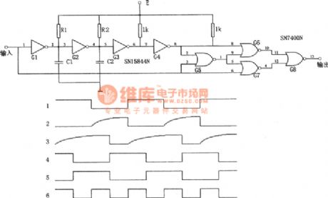
In the figure is the square wave doubler. In the circuit, gate G1 is the phaser inverter, the input signal crosses G1 and then in imposed on the input terminal of G2. When the voltage on the two terminals of C1 reaches the G2 threshold voltage, the output of G2 becomes logic 0 , at the moment, C2 discharges with the help of G2. When the input signal comes back to logic 1 , C1 is discharging with the help of G1 and C2 is charged by R2. When the voltage on the two terminals of C2 reaches the threshold voltage, the output of G3 becomes logic 0 . The NAND of G5, G6, 67 and G8 composes the OR gate. (View)
View full Circuit Diagram | Comments | Reading(843)
The 3-phase signal generator
Published:2011/6/21 9:49:00 Author:Borg | Keyword: 3-phase, signal generator
View full Circuit Diagram | Comments | Reading(1290)
The 3-phase square wave generator
Published:2011/6/21 10:00:00 Author:Borg | Keyword: 3-phase, square wave
View full Circuit Diagram | Comments | Reading(1304)
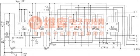
The 3-phase square wave signal oscillator
Published:2011/6/22 0:58:00 Author:Borg | Keyword: 3-phase, square wave, signal oscillator
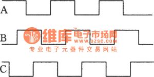
In the circuit is a gundam senary counter which is composed of a CD4017, the input clock frequency is 300Hz, VDl~VD9 and R1~R3 compose 3 s-phase input OR gates, they pick out the 3-phase square wave signals whose difference is 120o and the frequency is 50Hz. The 3-phase signal can be got from either A, B or C. The waveform are shown here.
(View)
View full Circuit Diagram | Comments | Reading(1375)
The SAFl032F infrared remote control receiving decoding circuit
Published:2011/6/19 10:19:00 Author:Seven | Keyword: infrared, remote control
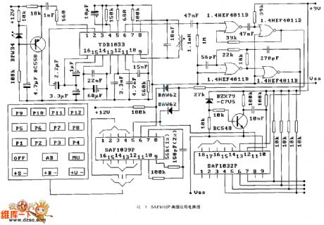
The SAFl032F typical application circuit (View)
View full Circuit Diagram | Comments | Reading(446)
The inverting power supply output circuit of the sine wave intermediate frequency
Published:2011/6/20 10:51:00 Author:Seven | Keyword: inverting power supply, output circuit, intermediate frequency
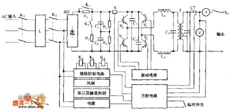
The inverting power supply output circuit of the sine wave intermediate frequency
(View)
View full Circuit Diagram | Comments | Reading(453)
The toy car circuit controlled by the color TV remote control
Published:2011/6/23 2:19:00 Author:qqtang | Keyword: toy car, color TV, remote control
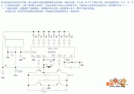
I reinstalled a toy car which can be used by the color TV remote control, the circuit is shown in the figure. P10~P17 connect with the lighting pipe as the 8-gear display; P3.5 and P3.7 control the advance of retreat of the motor, and the two can be in the low LEV at the same time, and they output a PWM square wave whose period is 80mS. The triode power is decided by the motor current. The keys of + and - control the heading direction, the sound volume key is used to control the speed, the power supply key is to control the pulling over of the toy car. The control distance is 18 meters, and it can be shaded by furnitures.
(View)
View full Circuit Diagram | Comments | Reading(747)
The simple circuit of long-distance control
Published:2011/6/22 6:55:00 Author:qqtang | Keyword: simple circuit, long-distance control
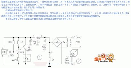
The principles and manufacturing process are as follows:The infrared receiver REM can be the general integral infrared receiver, the outline is shown in figure 1, the infrared remote signal received by REM is then magnified by V1 and V2 and pushes the infrared emitting pipe to work. In the figure, the part out of the hidden line is installed in the lounge room, after the infrared emitting diode is connected with the receiving part by the coaxial-cable, it is set in a hidden place in front of the satellite TV set in the living room. With this equipment, it is convenient for people to watch TV with the remote control in their hands.
(View)
View full Circuit Diagram | Comments | Reading(561)
The soft-starting control signal generating circuit
Published:2011/6/20 21:17:00 Author:Seven | Keyword: soft-starting, control signal
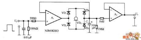
See as the figure, this is a soft-starting control signal generating circuit, it is used in the output voltage soft-starting of the power supply circuit , the signal source is controlled by the control signal or the motor with little mechanical shock. The output current of constant current diode VD5 charges CI and gets a linear rising/dropping waveform. A1 and A2 are the FET input computing amplifier NJM082BD whose bias current is low. The circuit linear rising signal is compared with the triangular wave by the comparator, then the wide pulse modulation PWM signal is generated.
(View)
View full Circuit Diagram | Comments | Reading(468)
The 3-phase sine signal generator circuit
Published:2011/6/20 22:39:00 Author:Seven | Keyword: 3-phase, sine signal
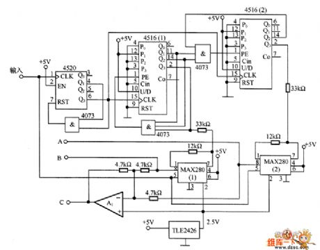
In the figure is the 3-phase sine signal generator circuit. This kind of circuit is widely used, such as controlling the voltage of the synchronized motor rotor. In the circuit, 2 dual-counters 4516(1)and 4516(2) with the low-pass filters MAX280(1) and MAX280(2) generate the phase-A and phase-B signals of sine waveform, and the signals are added together by A1 and then there generates an inverting phase signal of C. To reduce the distortion of the waveform, the counter outputs symmetric signals, and the phase different would better be 120°.
(View)
View full Circuit Diagram | Comments | Reading(3814)
The working principle circuit of the infrared remote control mouse
Published:2011/6/23 2:41:00 Author:qqtang | Keyword: working principle, remote control
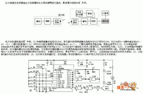
The infrared remote control mouse consists of the infrared emitter and receiver, whose principle circuit is shown in the figure. The infrared emitter is shown in the figure. IC1 is the encoder integrated circuit VD5026, and it is coupled with VD5027 and VD5028. The 1~8-pin of VD5026 are the address terminals A0~A7, 10~13-pin are the data terminals D0~D3 (when working with VD5028, they can be the address terminals A8~A11), 17-pin is the output terminal of the encoding signal, and its output signal modulates the signals of the 40KHz pulse generator composed of IC2A and IC2D.
(View)
View full Circuit Diagram | Comments | Reading(983)
| Pages:162/195 At 20161162163164165166167168169170171172173174175176177178179180Under 20 |
Circuit Categories
power supply circuit
Amplifier Circuit
Basic Circuit
LED and Light Circuit
Sensor Circuit
Signal Processing
Electrical Equipment Circuit
Control Circuit
Remote Control Circuit
A/D-D/A Converter Circuit
Audio Circuit
Measuring and Test Circuit
Communication Circuit
Computer-Related Circuit
555 Circuit
Automotive Circuit
Repairing Circuit