Signal Processing
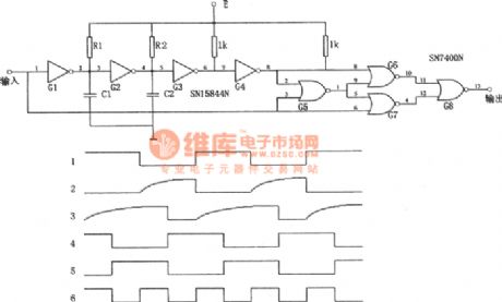
The square wave doubler (SN15844N and SN7400N)
Published:2011/6/17 19:51:00 Author:Borg | Keyword: square wave doubler | From:SeekIC

In the figure is the square wave doubler. In the circuit, gate G1 is the phaser inverter, the input signal crosses G1 and then in imposed on the input terminal of G2. When the voltage on the two terminals of C1 reaches the G2 threshold voltage, the output of G2 becomes logic 0 , at the moment, C2 discharges with the help of G2. When the input signal comes back to logic 1 , C1 is discharging with the help of G1 and C2 is charged by R2. When the voltage on the two terminals of C2 reaches the threshold voltage, the output of G3 becomes logic 0 . The NAND of G5, G6, 67 and G8 composes the OR gate.
Reprinted Url Of This Article:
http://www.seekic.com/circuit_diagram/Signal_Processing/The_square_wave_doubler_SN15844N_and_SN7400N.html
Print this Page | Comments | Reading(3)

Article Categories
power supply circuit
Amplifier Circuit
Basic Circuit
LED and Light Circuit
Sensor Circuit
Signal Processing
Electrical Equipment Circuit
Control Circuit
Remote Control Circuit
A/D-D/A Converter Circuit
Audio Circuit
Measuring and Test Circuit
Communication Circuit
Computer-Related Circuit
555 Circuit
Automotive Circuit
Repairing Circuit
Code: