
Signal Processing
Index 181
Friendship brand BCD-200 fridge circuit
Published:2011/5/9 9:09:00 Author:Christina | Keyword: Friendship, fridge circuit

The Friendship brand BCD-200 fridge circuit is as shown:
(View)
View full Circuit Diagram | Comments | Reading(597)
Yellow River BCD-170 type fridge circuit
Published:2011/5/9 9:10:00 Author:Christina | Keyword: Yellow River, fridge circuit

The Yellow River BCD-170 type fridge circuit is as shown:
(View)
View full Circuit Diagram | Comments | Reading(380)
Antarctic brand direct cooling type fridge circuit
Published:2011/5/9 6:11:00 Author:Christina | Keyword: Antarctic brand, direct cooling


The Antarctic brand direct cooling type fridge circuit are as shown:
(View)
View full Circuit Diagram | Comments | Reading(518)
FengHua brand BYD-175 type fridge circuit
Published:2011/5/9 8:03:00 Author:Christina | Keyword: FengHua, fridge circuit

The FengHua brand BYD-175 type fridge circuit is as shown:
(View)
View full Circuit Diagram | Comments | Reading(404)
Great Wall brand BCD-170, BCD-185 type fridge circuit
Published:2011/5/9 8:02:00 Author:Christina | Keyword: Great Wall, fridge circuit

The Great Wall brand BCD-170, BCD-185 type fridge circuitis as shown:
(View)
View full Circuit Diagram | Comments | Reading(484)
Great Wall brand BCD-160 type fridge circuit
Published:2011/5/9 8:00:00 Author:Christina | Keyword: Great Wall, fridge circuit

The Great Wall brand BCD-160 type fridge circuit is as shown in the figure:
(View)
View full Circuit Diagram | Comments | Reading(423)
General brand ER-20 type fridge circuit
Published:2011/5/9 7:59:00 Author:Christina | Keyword: General brand, fridge circuit

The General brand ER-20 type fridge circuit is as shown:
(View)
View full Circuit Diagram | Comments | Reading(429)
The Wiring Circuit(b) of Volga 3102
Published:2011/5/10 0:30:00 Author:Borg | Keyword: Wiring Circuit, Volga

As shown in figure 8 is the wiring circuit(b) of Volga 3102
21-clock; 22-rear window heating indicator; 30-speed-mileage light; 24- high beam indicator; 25-steering lamp; 26-fog lamp; 27- water thermometer; 28-instrument lamp; 29-engine temperature lamp; 30-hand brake indicator; 31-stand-by indicator; 32-brake failure indicator; 33-low oli pressure indicator; 34-oil pressure gauge; 35-oil lack indicator; 36-petrol gauge; 37-ignition switch; 38-flasher; 39-steering and headlight switch; 40-danger alarm switch; 41- heating switches of rear window;42-the cigar-lighter
60-fog lamp relay; 61-fog lamp switch;62-rear fog lamp; 63-rear fog indicator;64-fuse; 65-light lamp; 66-right fuse box; 67-parking lamp switch;68- back-up lamp switch;69-left fuse box; 70-headlight relay;71- current indicator (View)
View full Circuit Diagram | Comments | Reading(950)
The Wiring Circuit(c) of the Volga 3102 Car
Published:2011/5/10 3:36:00 Author:Borg | Keyword: Wiring Circuit, Volga 3102

As shown in Figure 9 is the wiring circuit of the Volga 3102 Car.
43-right door lamp; 44-left door lamp; 45-petrol sensor; 46-hand brake switch; 47-rear turing lamp; 48-rear width lamp; 49-brake lamp; 50-back-up lamp; 51-rear fog lamp; 52-ceiling lamp; 53-ceiling lamp switch; 54-warm wingd motor; 55-fan switch; 56-rear heating window; 57-license plate lamp; 58-baggage chamber lamp; 59-staff box lamp; 60-fog lamp relay (View)
View full Circuit Diagram | Comments | Reading(423)
CCD Analog Output Signal Processing Circuit
Published:2011/5/7 7:18:00 Author:Joyce | Keyword: CCD, Analog Output, Signal, Processing

AD623 integrates three op-amps, and it can work with either single power supply or dual power supply.It has relatively high CMRR and extremely low voltage drift. Except a external resistance which is used tocontrol programmable gain, all the other components are integrated in the interior, so as to improve the circuit`s temperature stability and reliability. The analog signal processing circuit of CCD applying AD623 is as shown in the graph.It can send video signals and compensating output to the inverted and non-inverting input of AD623 respectively.Connecting a first-level emitter follower to the output end of AD623 is to enhance the drive ability of the signals . This device can eliminate temperature drift of output signals in circuits using ordinary op-amps and peripheral resistance . (View)
View full Circuit Diagram | Comments | Reading(1137)
High Accuracy 50Hz Time Base Circuit
Published:2011/5/9 5:12:00 Author:Sue | Keyword: High Accuracy, 50Hz, Time Base


As seen in the figure is the high accuracy 50Hz time base circuit. It consists of two CMOS digital integrated circuits and quartz crystal. This circuit can generate 50Hz time base signal with an accurate frequency and consistent duty ratio. It is simple and easy to make. The figure below is the waveform figure.
(View)
View full Circuit Diagram | Comments | Reading(785)
Keying Oscillator Circuit
Published:2011/5/9 5:10:00 Author:Sue | Keyword: Keying, Oscillator

As seen in the figure is keying oscillator circuit composed of monostable trigger CC4098, Four-2 input terminal and NOT gate CC4011. This circuit has a adjustable frequency and duty ratio. It is mainly usd in low frequency signal generator with a low accuracy requirement. (View)
View full Circuit Diagram | Comments | Reading(515)
Atmospheric Manometer Signal Regulating Circuit
Published:2011/5/9 5:21:00 Author:Sue | Keyword: Atmospheric Manometer, Signal Regulating

*1% thin film resistor, **0.1%thin film resistor, the type of T1 is NPH-8-100AH. (View)
View full Circuit Diagram | Comments | Reading(1146)
Using NE555 Skillfully as Linear Triangle Generator Circuit
Published:2011/5/6 11:24:00 Author:Joyce | Keyword: Using NE555 Skillfully as, Linear, Triangle Generator

Using NE555 Skillfully as Linear Triangle Generator Circuit (View)
View full Circuit Diagram | Comments | Reading(2422)
Signal Circuit of Duty Ratio Ajustable Clock Consisting of 4 NAND gates
Published:2011/5/7 7:30:00 Author:Joyce | Keyword: Signal, Duty Ratio Ajustable, Clock , Consisting of 4 NAND gates
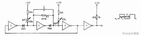
As shown in graph, the circuit is composedof four NAND gates. Oscillation signal frequency is decided by C and the value of potentiometer RP1. RP2 . Changing the resistance of potentiometer can change the frequency whose adjustment range can be 20:1.The resistance of potentiometer RP2 sets the width of output waveform T1 ,and the resistance of potentiometer RP2 sets the width of the output waveform T2.
(View)
View full Circuit Diagram | Comments | Reading(523)
MAX2l01-digital satellite receiving IF signal processing integrated circuit diagram
Published:2011/5/6 21:27:00 Author:Nicole | Keyword: digital satellite, receiving, IF signal processing

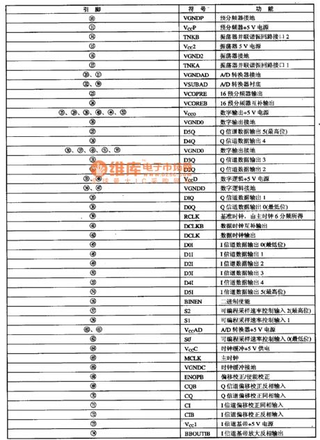
MAX2l01 is a digital satellite receiver special IF signal processing and A/D transformation single chip larger scale integrated circuit which is produced by MAXIM Company.
1, functions and features
MAX2l01 integrated circuit's sampling rate is 6OMb/S, it contains voltage controlled oscillator which is used for I/Q channel demodulator, orthogonal generator network, 16 prescaler which is used for phase locking loop oscillator, the changeable sampling rate programmable counter has the function of: signal detection and automatic baseband migration elimination. MAX2l01 receives narrow band medium frequency input singal, the center frequency is located between 400-700 MHz UHF frequency band. The typical application circuit of this integrated block is shown in the figure1.
The figure1 is the application circuit of MAX2l01 integrated block
2, pin function
MAX2l01 integrated circuit adopts 100-foot package, the pin function of this integrated circuit is shown in the table1.
The table1 is the pin function of MAX2l01 integrated circuit
(View)
View full Circuit Diagram | Comments | Reading(1481)
U3660M B IH baseband chrominance signal delay line integrated circuit
Published:2011/5/9 2:07:00 Author:Nicole | Keyword: baseband, chrominance signal, delay line
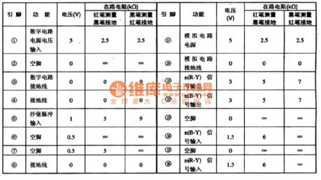
U3660M-B is a IH baseband chrominance signal delay line integrated circuit, it is used as adjusting-free baseband chrominance signal process, it is suitable for decode circuit with ±(R-Y)、±(B-Y) chrominance signal output, it is applied to TOSHIBA series large screen color television.
1. functions and features
U3660M-B integrated bolck contains two groups: one part is two comb filters which adopt switched capacitor switching technique 64μs delay time, the other part is 3MHz clock generator circuit.
2. pin function and data
The pin function and data of U3660M-B integrated circuit is shown in the table1-1.
(View)
View full Circuit Diagram | Comments | Reading(233)
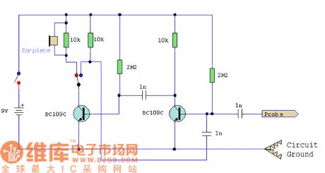
Signal tracing device circuit diagram
Published:2011/5/6 1:44:00 Author:Ecco | Keyword: Signal , tracing device
View full Circuit Diagram | Comments | Reading(481)
CM0006CF digit convergence singal process integrated circuit diagram
Published:2011/5/6 8:28:00 Author:Nicole | Keyword: digit convergence, singal process
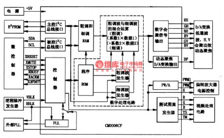
CM0006CF is a digit convergence singal process special integrated circuit, it is a rear projection TV special chip, such as Changhong 51PT28A rear projection, it adopts this integrated circuit.
1, functions and features
CM0006CF integrated circuit contains row, field scanning singal position sampling circuit, A/D converter, field scanning waveform correction generator, row scanning waveform correction generator and combination operational circuit. It has multiple scanning format (PAL/NTSC/HDTV、interlaced scanning/progressive scanning、VGA), 6bit digital output terminal are used to convergence correct, a simulated output terminal is used to dynamic focusing, two 8bit width regulation pulse output terminal, besides, convergence correction uses the production function of grid image, order diagram and cursor. The internal circuit block diagram of this integrated block is shown in the figure1.
The figure1 is the internal circuit block diagram of CMO006CF integrated block
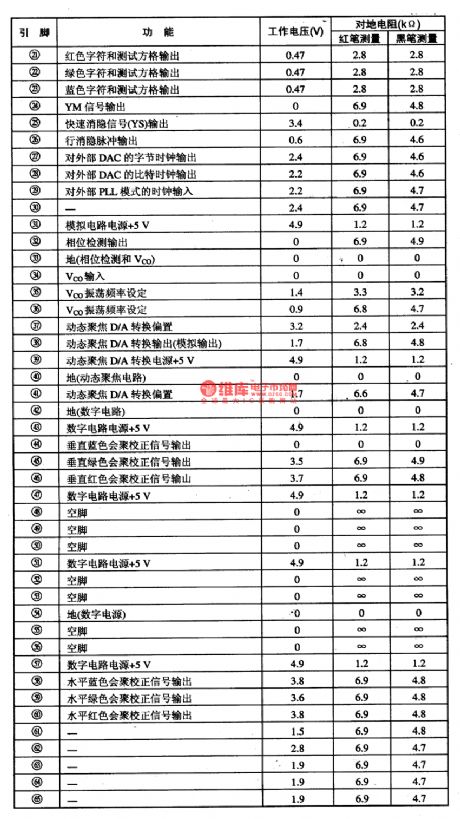
2, pin function and data
The pin function and data of CMO006CF integrated circuit is shown in the table1.
The table is the pin function and data of CMO006CF integrated circuit (View)
View full Circuit Diagram | Comments | Reading(539)
LMl269NA-video signal pretreatment integrated circuit diagram
Published:2011/5/6 2:11:00 Author:Nicole | Keyword: video signal, pretreatment
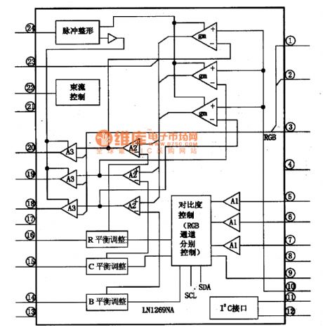
LMl269NA is a video signal pretreatment integrated circuit which is produced by National Semiconductor Corporation, it is widely used in new type computer display, such as QINGHUA TONGFANG 5E color display.
1, internal circuit block diagram
LMl269NA integrated circuit contains R, G, B three primary colors balance adjusting circuit, pulse shaping circuit, beam current control circuit, contrast ratio control circuit I square C interface circuit and other assistant functions circuits. The internal circuit block diagram of manifold block is shown in the figure1.
The figure1 is the internal circuit block diagram of manifold block LMl269NA.
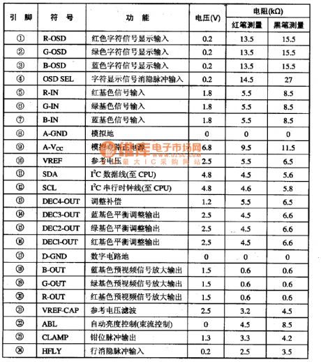
LMl269NA integrated circuit adopts knife-foot dual in-line package, the pin function and data of this integrated circuit is shown in the table1, the data measures TSINGHUA TONGFANG 5E color display, the display pattern is 800X600.
The table1 is the pin function and data of LMl269NA integrated circuit.
(View)
View full Circuit Diagram | Comments | Reading(674)
| Pages:181/195 At 20181182183184185186187188189190191192193194195 |
Circuit Categories
power supply circuit
Amplifier Circuit
Basic Circuit
LED and Light Circuit
Sensor Circuit
Signal Processing
Electrical Equipment Circuit
Control Circuit
Remote Control Circuit
A/D-D/A Converter Circuit
Audio Circuit
Measuring and Test Circuit
Communication Circuit
Computer-Related Circuit
555 Circuit
Automotive Circuit
Repairing Circuit