
Signal Processing
Index 161
Simple doubler generator
Published:2011/6/19 2:59:00 Author:Lucas | Keyword: Simple, doubler, generator
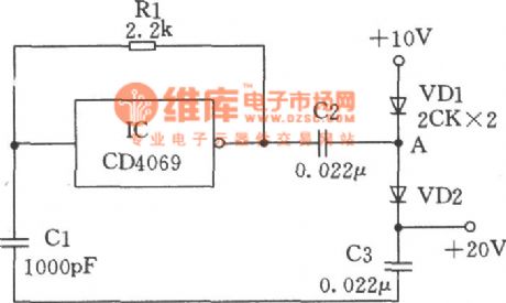
The simple doubler circuit composed of CMOS NOT gate is shown as the chart. The IC in the chart is the inverter and the inverter, Rl, Cl form a square wave oscillator with the frequency about l00kHz, and the oscillator output changes between 0 ~ 10V. When the output is 0V, the capacitor charges to 10V by VD1, when oscillator output changes into +10 V from 0V in a sudden, because the voltage across the capacitor can not change suddenly, the A end of capacitor C2 should be improved accordingly to +20 V, then VDl is reverse-biased, and the current through the VD2 charge to C3, so the output end gets +20 V voltage. But taking into account the diode has voltage drop, so the actual output is slightly lower than +20 V.
(View)
View full Circuit Diagram | Comments | Reading(608)
Pocket television signal generator
Published:2011/6/21 5:33:00 Author:Lucas | Keyword: Pocket, television , signal generator
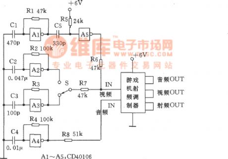
The television signal generator composed of a game RF modulator and a piece of CMOS integrated circuit is shown as the chart. In the Figure: Schmitt triggers Al ~ A4 and RC components form the line sync, horizontal, vertical, and audio signal oscillator. S is used to select the horizontal, vertical signal. A5 and differential circuit C5, R5 will shape the line sync signal in 5 ~ 7μs positive narrow pulse, which will be sent into the RF modulator with horizontal, vertical signal. The power can use the 6V cascading battery.
(View)
View full Circuit Diagram | Comments | Reading(496)
Three-phase waveform generator composed of CD4017
Published:2011/6/20 6:13:00 Author:Lucas | Keyword: Three-phase , waveform , generator
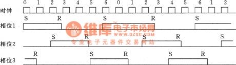
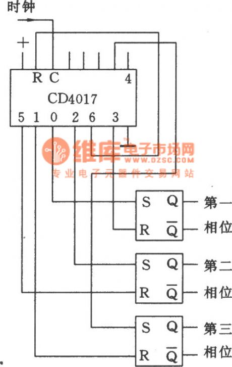
The circuit shown as the chart can use single-phase square wave three-phase to produce square wave, and the three-phase output frequency range is only limited by the logic capacity. Output frequency is 1 / 6 of the input frequency. As bistable flip-flop can change the waveform, the actual input waveform may not be square wave. In the figure, CD4017 is the decimal output CMOS counter with reset function. When the counting resets to 6:00, and then starts counting to six.
(View)
View full Circuit Diagram | Comments | Reading(4358)
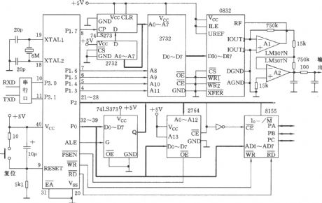
Multi-road phase shift signal generator
Published:2011/6/20 8:20:00 Author:Lucas | Keyword: Multi-road , phase shift, signal generator
View full Circuit Diagram | Comments | Reading(484)
Seconds signal generator composed of CC4060
Published:2011/6/20 8:22:00 Author:Lucas | Keyword: Seconds, signal generator
View full Circuit Diagram | Comments | Reading(450)
Seconds signal processing circuit(CC4518,CC4001)
Published:2011/6/20 8:25:00 Author:Lucas | Keyword: Seconds , signal processing
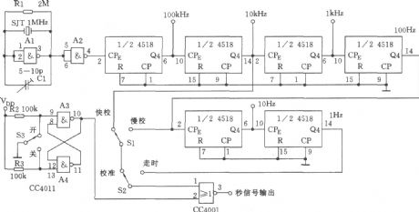
View full Circuit Diagram | Comments | Reading(509)
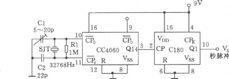
Precise second pulse signal generator
Published:2011/6/20 8:30:00 Author:Lucas | Keyword: Precise , second, pulse signal, generator

View full Circuit Diagram | Comments | Reading(611)
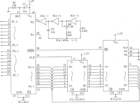
Programmable signal generator composed of 8031 SCM
Published:2011/6/20 8:18:00 Author:Lucas | Keyword: Programmable , signal generator, SCM
View full Circuit Diagram | Comments | Reading(659)
The oscillator circuit composed of frequency integrator circuits
Published:2011/6/23 10:31:00 Author:qqtang | Keyword: oscillator circuit, frequency integrator
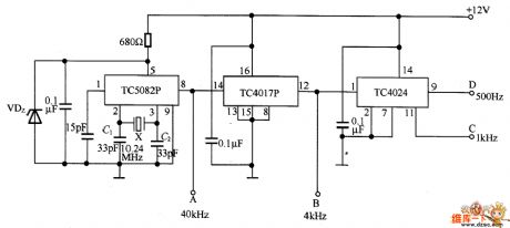
In the figure is the oscillator circuit composed of frequency integrator circuits. In the circuit, X is the 10.24MHz crystal oscillator. TC5082P contains a 12-stage frequency splitter, which is widely used. The former oscillating frequency 10.24MHz is split by TC5082P, the 7-pin outputs 10KHz, 6-pin outputs 5KHz, 4-pin outputs 2.5KHz and 8-pin outputs 40KHz, i.e A terminal outputs 40KHz. After being split by TC10I7P, the 12-pin(B terminal) outputs 4KHz, and then split TC4024, 11-pin (C) outputs 1KHz, 9-pin(D) outputs 500Hz, etc. The oscillating frequency can be trimmed by changing C1 and C2.
(View)
View full Circuit Diagram | Comments | Reading(565)
The frequency multiplier circuit
Published:2011/6/22 6:27:00 Author:qqtang | Keyword: frequency multiplier
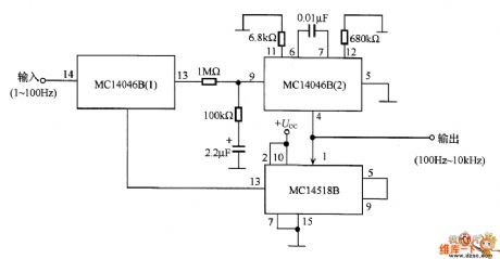
In the figure is the frequency multiplier circuit, the output signal frequency is 100 times of the input one, the frequency range is 1~100Hz. In the circuit, the phaser is MC14046B (1), the voltage control oscillator is MC14046B (2). The voltage control oscillator does the 100 frequency splitting with the 2-bit decimal counter inside it, and the output signal is compared with the input signal which makes the phase synchronize.
This circuit is used to precisely count the low frequency signals which are generated by living organisms in a short time, or used in control pulses of power control acquirement and power supply frequency synchronization. (View)
View full Circuit Diagram | Comments | Reading(2252)
The high speed reaction differential pulse generating circuit
Published:2011/6/23 21:01:00 Author:Seven | Keyword: high speed reaction, differential pulse
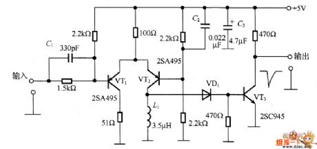
In the circuit, the transistor VT1 and VT2 compose the difference amplifier circuit, to raise the reaction speed, the circuit works in non-saturation state. If the input pulse is 0~+5V, the collecting electrode current is higher than TV2 when it is 0V, if the input is +5v, then the collecting electrode current of VT2 is rising quickly, and the differential waveform is got by L1. VD1 is the Schottky diode of high speed switch, which only allows the forward waveform to conduct VT3. Its basic pole current flows in VT3, then there is collecting electrode current, the LEV is falling quickly and generates a passive differential pulse.
(View)
View full Circuit Diagram | Comments | Reading(866)
The oscillating frequency mixer circuit
Published:2011/6/19 20:21:00 Author:qqtang | Keyword: oscillating frequency
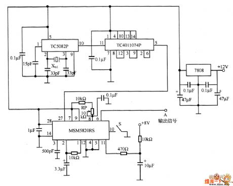
When the required frequency stabilization is high, the oscillator is often made of crystal, because the crystal temperature character is very high. In fact, we often need the improved high-stabilization oscillating circuit, that's why we need to fine-tune the oscillating frequency, and the temperature character is the same when the frequency reaches some values. It's not enough to choose the crystal, therefore, we can use phase-lock PLL frequency mixer. See as the figure, this is the frequency mixer, the chip of the mixer is MSM5820RS.
(View)
View full Circuit Diagram | Comments | Reading(649)
The sine wave output circuit
Published:2011/6/23 20:09:00 Author:Seven | Keyword: sine wave, output
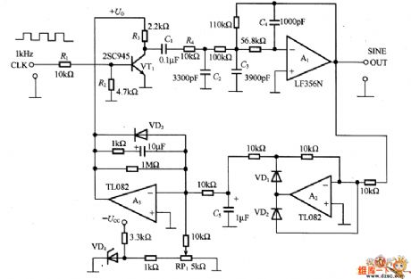
In the circuit, VT1 is the AM circuit, it switches the control voltage +UG with a 1KHz clock signal and generates square wave, then the high frequency harmonic wave is filtered by the low-pass filter. R4 and C2 are used to set the flat time constant of the wave front edge, A1 is the buffer amplifier. The half-wave output by A1 is rectified by the ideal diode which is composed by A2, and C5 smooths the rectifier output, and the output is compared with the VD4 reference voltage, if it is higher than the Vref, then the output of A3 is dropping and UG on VT1 is falling.
(View)
View full Circuit Diagram | Comments | Reading(712)
The ladder wave signal generating circuit
Published:2011/6/23 20:50:00 Author:Seven | Keyword: ladder wave, signal generating

In the figure is the ladder wave signal generating circuit. In the circuit, 74HC193 is a 4-bit binary counter, on the output terminal connects with a R-2R resistor ladder net, which composes a 4-bit D/A converter. The 15th stage voltage is the total value of all the 5V power supply, i.e 5V×15/16=4.6875V, the voltage on each stage is 312.5mV. To make the maximum voltage 10V, A1 magnifies it to its twice, if the voltage on each stage is not suitable in usage, the voltage can be split on its output terminal.
(View)
View full Circuit Diagram | Comments | Reading(1140)
The short pulse string waveform generating circuit
Published:2011/6/23 20:26:00 Author:Seven | Keyword: short, pulse string, waveform
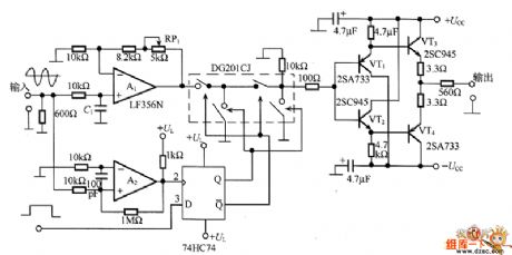
In the figure is the short pulse bundle waveform generating circuit.
A2 is the comparator, which detect the positive zero crossing point, and it outputs short pulse wave strings from sin0°, and the wave string is synchronized by 74HC74. The output time of the short pulse string is provided by the external pulse generator, but this will make it not synchronize with the phase of the sine wave oscillator, so when it reaches the high LEV with the help of the short control pulse, it makes the Q point of the dual stable state multi-resonance oscillator 74HC74 in a high LEV, then analog switch DG201CJ is on and the pulse string is output by the buffer. (View)
View full Circuit Diagram | Comments | Reading(547)
The low frequency sawtooth wave generating circuit
Published:2011/6/23 20:38:00 Author:Seven | Keyword: low frequency, sawtooth wave
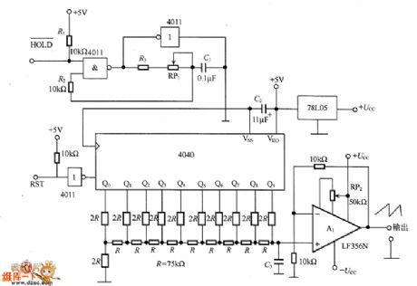
In the figure is the low frequency sawtooth wave generating circuit. The circuit consists of the clock oscillator 4011, IO bit counter 4040, R2-R resistor ladder network, reference voltage generator 78LO5, buffer amplifier A1 and so on. The output wave is a ladder wave which splits the 0~10v into 1024 pieces equally(about 10mV). When the frequency is constant, the rising time can be prolonged by adding C3 and gets a smooth waveform.
(View)
View full Circuit Diagram | Comments | Reading(1956)
The NE555 sawtooth wave generator circuit
Published:2011/6/23 21:21:00 Author:Seven | Keyword: sawtooth wave, generator
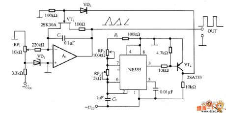
Sawtooth waves can be used as the scanning signal, which are often acquired by capacitor discharging. This circuit maximizes the output voltage and frequency change by changing the reset timing of the integral circuit. In the circuit, A1 is the integrator, when the power is on, A1 is starting to integrating with the set current, when the current reaches the VT1 threshold, VT1 is conducting, the electricity of C1 is released by VT1, after the reset signal is cancelled, the charge is started again, NE555 will output the reset pulse in T=0.693C2(R1+RP2+RP3).
(View)
View full Circuit Diagram | Comments | Reading(1901)
The ultrasonic wave emitting and receiving circuit
Published:2011/6/17 1:07:00 Author:Seven | Keyword: ultrasonic wave, emitting and receiving
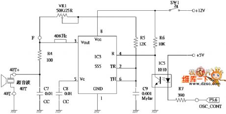
View full Circuit Diagram | Comments | Reading(480)
The infrared wireless headphone circuit
Published:2011/6/19 0:24:00 Author:Seven | Keyword: wireless headphone
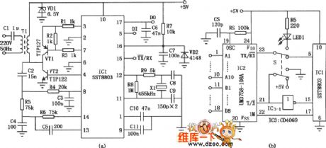
As the inductive wireless headphone emitter must be fixed on the wall or the ceiling of the room, it can't be used outside, which is the weakness of inductive wireless headphones. But the infrared wireless headphone is different, as its signal is emitted by a portable infrared emitting circuit, which can not only be used in e-teaching, domestic TV and stereo equipment audio signal wireless reception, but also used in outdoor portable radios, CD, VCD and MP3 without wires, so it is a real walkman .
(View)
View full Circuit Diagram | Comments | Reading(1583)
The random frequency doubler composed of CH7555
Published:2011/6/17 7:23:00 Author:Borg | Keyword: random frequency doubler
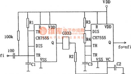
Usually, the frequency doubler composed of phase-lock loop has good functions, and it can get a high frequency multiply ratio, but the construction of the circuit is complex and it's costly. However, the homogenization of the output which is generated in the method of edge detection is bad. The figured circuit characterizes simpleness, wide dynamic range, good homogenization and so on. In the figure, the CH7555 timer is converted into a common multi-resonance oscillator on the right side, the rising of the control voltage will lead to the dropping of the output frequency. The input reaches the single stable circuit firstly. (View)
View full Circuit Diagram | Comments | Reading(672)
| Pages:161/195 At 20161162163164165166167168169170171172173174175176177178179180Under 20 |
Circuit Categories
power supply circuit
Amplifier Circuit
Basic Circuit
LED and Light Circuit
Sensor Circuit
Signal Processing
Electrical Equipment Circuit
Control Circuit
Remote Control Circuit
A/D-D/A Converter Circuit
Audio Circuit
Measuring and Test Circuit
Communication Circuit
Computer-Related Circuit
555 Circuit
Automotive Circuit
Repairing Circuit