Signal Processing
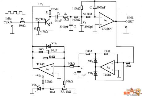
The sine wave output circuit
Published:2011/6/23 20:09:00 Author:Seven | Keyword: sine wave, output | From:SeekIC

In the circuit, VT1 is the AM circuit, it switches the control voltage +UG with a 1KHz clock signal and generates square wave, then the high frequency harmonic wave is filtered by the low-pass filter. R4 and C2 are used to set the flat time constant of the wave front edge, A1 is the buffer amplifier. The half-wave output by A1 is rectified by the ideal diode which is composed by A2, and C5 smooths the rectifier output, and the output is compared with the VD4 reference voltage, if it is higher than the Vref, then the output of A3 is dropping and UG on VT1 is falling.
Reprinted Url Of This Article:
http://www.seekic.com/circuit_diagram/Signal_Processing/The_sine_wave_output_circuit.html
Print this Page | Comments | Reading(3)

Article Categories
power supply circuit
Amplifier Circuit
Basic Circuit
LED and Light Circuit
Sensor Circuit
Signal Processing
Electrical Equipment Circuit
Control Circuit
Remote Control Circuit
A/D-D/A Converter Circuit
Audio Circuit
Measuring and Test Circuit
Communication Circuit
Computer-Related Circuit
555 Circuit
Automotive Circuit
Repairing Circuit
Code: