Signal Processing
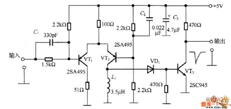
The high speed reaction differential pulse generating circuit
Published:2011/6/23 21:01:00 Author:Seven | Keyword: high speed reaction, differential pulse | From:SeekIC

In the circuit, the transistor VT1 and VT2 compose the difference amplifier circuit, to raise the reaction speed, the circuit works in non-saturation state. If the input pulse is 0~+5V, the collecting electrode current is higher than TV2 when it is 0V, if the input is +5v, then the collecting electrode current of VT2 is rising quickly, and the differential waveform is got by L1. VD1 is the Schottky diode of high speed switch, which only allows the forward waveform to conduct VT3. Its basic pole current flows in VT3, then there is collecting electrode current, the LEV is falling quickly and generates a passive differential pulse.
Reprinted Url Of This Article:
http://www.seekic.com/circuit_diagram/Signal_Processing/The_high_speed_reaction_differential_pulse_generating_circuit.html
Print this Page | Comments | Reading(3)

Article Categories
power supply circuit
Amplifier Circuit
Basic Circuit
LED and Light Circuit
Sensor Circuit
Signal Processing
Electrical Equipment Circuit
Control Circuit
Remote Control Circuit
A/D-D/A Converter Circuit
Audio Circuit
Measuring and Test Circuit
Communication Circuit
Computer-Related Circuit
555 Circuit
Automotive Circuit
Repairing Circuit
Code: