
Basic Circuit
Index 291
10_kH_GYRATOR
Published:2009/7/2 4:58:00 Author:May
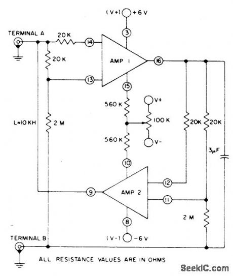
Active filter circuit uses two sections of CA3060 three-opamp array as gyrator that makes 3-μF capacitor function as fioating 10-kilohenry inductor across terminals A and B, Q of inductor is 13. l00k pot tunes inductor by changing gyration resistance.- Linear Integrated Circuits and MOS/FET's, RCA Solid State Division, Somerville, NJ, 1977, p 152. (View)
View full Circuit Diagram | Comments | Reading(1180)
HV_REGULATOR_WITH_FOLDBACK_CURRENT_LIMITING
Published:2009/7/2 4:57:00 Author:May
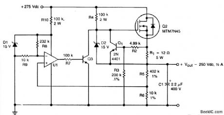
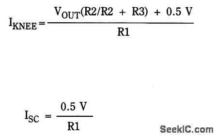
Circuit NotesA TMOS MTM7N45 (Q2) is used as a series pass element in a linear high voltage supply that accepts +275-V unregulated and produces 250 V regulated with foldback current limiting.A 15-V zener, D1, provides the dc reference for operational amplifier U1, whose other input is obtained from a fraction of the output voltage. UI drives Q3, which drives the gate of Q2. Foldback current limiting is achieved by RI, R2, R3, R4, Q1, and D2. The formula to estab!ish the current knee for limiting is:
(View)
View full Circuit Diagram | Comments | Reading(1310)
15_kHz_NOTCH
Published:2009/7/2 4:57:00 Author:May
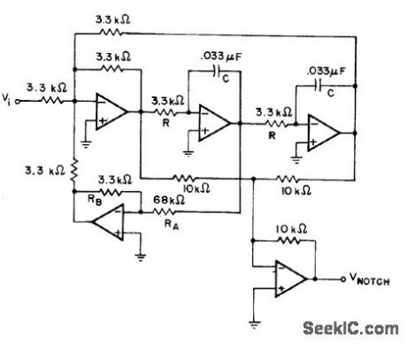
Unity-gain state-variable filter consists of low-pass and high-pass sections combined with two-input summing amplffierto give notch response for suppression of 1.5-kHz signals. Opamps can be 741.-H. M. Berlin, Design of Active Filters, with Experiments, Howard W. Sams, Indianapolis, IN, 1977, p 186-189. (View)
View full Circuit Diagram | Comments | Reading(677)
GLOW_PLUG_DRIVER
Published:2009/7/2 4:56:00 Author:May
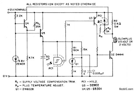
Model airplanes, boats, and cars use glow plug ignitions for their miniature (0,8cc to 15cc) internal combustion engines. Such engines dispense with the heavy on-board batteries, H.T. coil, and condenser required for conventional spark ignition, while simultaneously developing much higher RPM (hence power) than the compression ignition (diesel) motors. The heart of a glow plug is a platinum alloy coil heated to incandescence for engine starting by an external battery, either 1.5 volts or 2 volts. Supplementing this battery, a second 12-volt power supply is frequently required for the engine starter, together with a third 6 volt type for the electrical fuel pump.Rather than being burdened by all these multiple energy sources, the model builder would prefer to carry (and buy) a single 12-volt battery, deriving the lower voltages from this by use of suitable electronic step-down transformers (choppers). The glow driver illustrated does this and offers the additional benefit of (through negative feedback) maintaining constant plug temperature independent of engine flooding, or battery voltage while the starter is cranking.In this circuit, the PUT relaxation oscillator Q1 turns on the output chopper transistor Q2 at a fixed repetition rate determined by R1 and C1. Current then flows through the glow plug and the parallel combination of the current sense resistor R2 and the LED associated with the H11L Schmitt trigger. With the plug cold (low resistance), current is high, the H11L is biased on , and Q3 conducts to sustain base drive to Q2. Once the plug has attained optimum operating temperature, which can be monitored by its ohmic resistance, the H11L is programmed (viaRP).to switch off, removing base drive from Q3 and Q2.However, since the H11L senses glow plug current, not resistance, this is only valid if supply voltage is constant, which is not always the case. Transistor Q4 provides suitable compensation in this case; if battery voltage falls (during cold cranking, for instance), the collector current of Q4 rises, causing additional current to flow through the LED, thus delaying the switch-off point for a given plug current. The circuit holds plug temperature relatively constant, with the plug either completely dry or thoroughly wet , over an input voltage range of 8 to 16 volts. A similar configuration can be employed to maintain constant temperature for a full size truck diesel glow plug (28-volts supply, 12-volts glow plug); in this case, since plug temperature excursions are not so great, a hysteresis expansion resistor RH may be required. (View)
View full Circuit Diagram | Comments | Reading(3680)
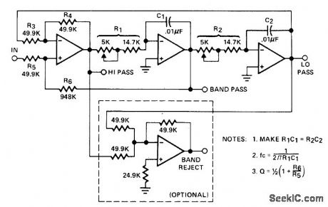
700_Hz_STATE_VARIABL_E
Published:2009/7/2 4:55:00 Author:May
Provides voltage gain at center frequency of 100 (40 dB) and Q of 50. Used when simultaneous low-pass, high-pass, and bandpass output responses are re quired. Cutoff frequency of low-pass and high-pass responses is equal to center frequency of bandpass response. Opamps can be 741. Based on use of 5% resistors.-H. M. Berlin, Design of Active Filters, with Experiments, Howard W.Sams,Indianapolis, IN, 1977, p 184-187. (View)
View full Circuit Diagram | Comments | Reading(500)
5_kHz_SERIES_SWITCHED_BANDPASS
Published:2009/7/2 4:54:00 Author:May
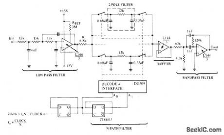
N-path filter having N of 4,Q of 500, and voltage gain of 2 uses DG5O9 four-channel CMOS differential multiplexer having necessary pairs of analog switches and decode logic. Dual D flip-flop generates 2-bit binaly sequence from 20-kHz clock signal. Bandwidth is about 10 Hz for 3 dB down, centered on 5 kHz.- Analog Switches and Their Applications, Siliconix, Santa Clara, CA, 1976, p 5-15-5-17. (View)
View full Circuit Diagram | Comments | Reading(490)
AF_NOISE_LlMlTER
Published:2009/7/2 4:53:00 Author:May

Operation is similar to that of delay line. Voltage developed across voltage divider at output of 1N34 germanium diode is instantaneous, while DC voltage at output of circuit is delayed. If no pulses are present and 0.1-μF capacitor is not at ground, 1N914 silicon diode will have floating voltage. High positive pulses charge capacitor, and silicon diode shorts audio voltage. Negative pulses disable germanium diode directly. Circuit thus acts as noise blanker in both directions. Used in European communication receivers. Transistor type is not criticaL-U. L. Rohde, IF Amplifier Design. Ham Radio, March 1977. p 10-21. (View)
View full Circuit Diagram | Comments | Reading(535)
1_kHz_STATE_VARIABLE_WITH_Q_OF_1O
Published:2009/7/2 4:53:00 Author:May
Use of all four sections of Harris HA-4602/4605 quadopamp glves four types of 1-kHz second-order filtering simultaneously.Pot adjustments permit matching of various RC products allowing for noninteractive adjustment of Q and center frequency.- Linear & Data Acquisition Products, Hamis Semiconductor, Melbourne, FL,vol,1,1977,p 2-84. (View)
View full Circuit Diagram | Comments | Reading(508)
10_20_kHz_BANDPASS
Published:2009/7/2 4:51:00 Author:May
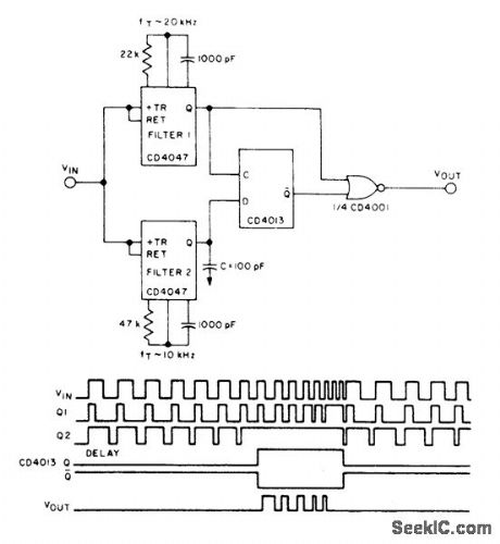
Two CD4047A lowpass filters, one connected for 10-kHz cutoff and other for 20-kHz cutoff, drive CD4013A flip-flop.If output of filter 2 is delayed by C, flip-flop clocks high only when input pulse frequency exceeds 10-kHz cutoff of filter 2. Waveforms show performance when input signal is swept through passband.- CQS/MOS Integrated Circuits, RCA Solid State Division, Somerville, NJ,1977,p 619. (View)
View full Circuit Diagram | Comments | Reading(589)
AUTOMOTIVE_EXHAUST_EMISSIONS_ANALYZER
Published:2009/7/2 4:49:00 Author:May
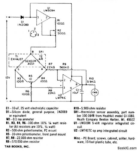
A bridge circuit contains two 100-ohm resistors (R3 and R4), and two thermistors (T1 and T2). At room temperature the resistance of T1 and T2 is about 2000 ohms. When they are each heated to 150℃ by a 10 mA current, the resistance value decreases to 100 ohms. Thus, the four elements comprise a bridge circuit. A characteristic of CO is that it conducts heat away from a thermistor at a different rate than air. One thermistor, T1, is exposed to the automobile exhaust while the other, T2, is isolated in a pure air environment. The difference in thermal conduction unbalances the bridge. A voltage difference is caused between points A and C. A differential amplifier, U1, amplifies this difference and drives the meter with sufficient current to read out the percentage of CO and the air-fuel ratio. A front panel balance control, R5, balances the bridge and calibrates the instrument. Calibration is performed when both thermistors are exposed to the outside air. (View)
View full Circuit Diagram | Comments | Reading(584)
NOISE_RESISTANT_LATCH
Published:2009/7/2 4:49:00 Author:May
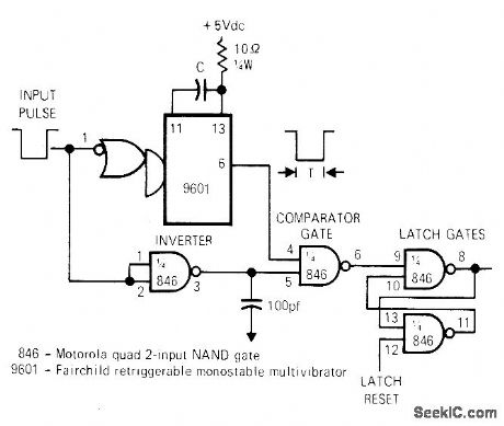
False triggering of latch gates by noise spikes is prevented by generating pulse T whose width is equal to minimum width of desired input pulse. Values used for RC combination set T. If R is chosen as 10 kilohms, C should be T/3.424, where C is in picofarads and T is in nanoseconds.-S. ft. Martin, Latching Circuit Provides Noise Immunity, EDN/EEE Magazine. Feb. 1. 1972. p 56. (View)
View full Circuit Diagram | Comments | Reading(512)
CURRENT_MODE_SCHMITT_TRIGGER
Published:2009/7/2 4:37:00 Author:May

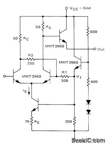
Motorola MMT3960 transistor array is connected as differential amplifier with feedback to produce Schmitt trigger having input hysteresis of 500 mV. Small rise and fall times make circuit suitable for driving flip-flop over wide range of frequencies.-B. Broeker, Micro-T Packaged Transistors for High Speed Logic Systems, Motorola, Phoenix, AZ, 1974, AN-536, p 6. (View)
View full Circuit Diagram | Comments | Reading(961)
MICROPOWER_HIGH_INPUT_IMPEDANCE_20_dB_AMPLIFIER
Published:2009/7/2 4:36:00 Author:May
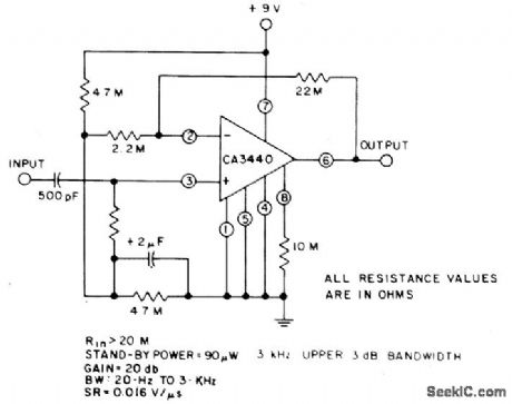
This circuit takes advantage of low power drain,high input impedance,and theexcellent frequency capability of the CA3440.Only a 500-pF input coupling capacitor is needed to achieve a 20 Hz, -3 dB low-frequency response. (View)
View full Circuit Diagram | Comments | Reading(504)
TWO_GATE_SCHMlTT
Published:2009/7/2 4:33:00 Author:May

TTL inverter gates are connected in series, with small feedback resistorin common ground lead, so gates are always in opposing logic states. Resulting constqnt voltage drop across 22-ohm resistor produces constant offset voltage that is corrected by 220-ohm resistor at output terminal. With values shown, positive-going threshold is 2.4 V and negative-going threshold is 2 V.-C. J. Ulrick, Schmitt Tdgger Uses Two Logic Gates, EEE Magazine, Dee. 1970, p 54. (View)
View full Circuit Diagram | Comments | Reading(576)
NOISE_GATE_FOR_AF_PREAMP
Published:2009/7/2 4:31:00 Author:May
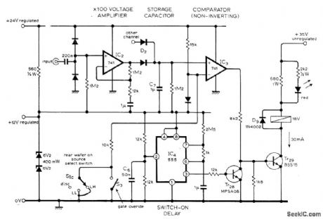
Used in highperformance phono preamplifier to mute output when there is no signal at phono input.Opamps each provide gains of about 100,Circuit controls muting reed relay serving both stereo channels of preamp. Delay switch-on using 555lC overrides noise-gate opamps. Unmarked diodes are 1 N914 or equivalent, and red LED is TIL209 or equivalent. Article covers circuit operation in detail and gives all other circuits of preamp.- D. Self. Advanced Preampli-fier Design, Wireless World, Nov 1976. p41-46. (View)
View full Circuit Diagram | Comments | Reading(846)
FOUR_CHANNEL_FOUR_TRACK_MIXER
Published:2009/7/2 4:25:00 Author:May
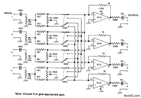
This circuit can be used as a stereo mixer as well as a four track. The quad op-amp IC gives a bit of gain for each track. The pan control allows panning between tracks one and two with the switch in the up position, and with the switch in the down position, it makes possible panning between tracks three and four. Extra channels can be added.A suitable op amp for IC1 is TL074 or similar. (View)
View full Circuit Diagram | Comments | Reading(1924)
15-3500_Hz_BANDPASS
Published:2009/7/2 4:25:00 Author:May
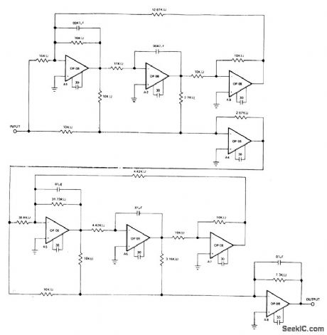
Five-pole telecommunication filter using eight Precision Monolithics op-08 opamps provides better than 30-dB attenuation in stop band.Total supply drain is only 4.8 mA for±15 V supply.- Precision Low Input Current Op Amp, Preoision Monolithics, Santa Clara, CA,1978,OP-08,p 6. (View)
View full Circuit Diagram | Comments | Reading(612)
10_kHz_VARIABLE_Q
Published:2009/7/2 4:22:00 Author:May
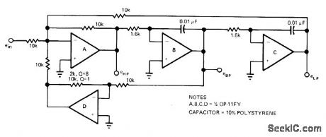
Second-order state-variable filter having center frequency of 10 kHz uses all four sections of opamp Center frequency can be tuned by varying 1.6K feedback resistors or by changing 0.01-μF feedback capacitors. Value of feedback resistor for opamp D determines Q of filter, for adjusting circuit bandwidth or damping. For higher-frequency operation, use high-speed opamps such as OP-15 or OP-16.-D. Van Dalsen, Need an Active Filter? Try These Design Aids, EDN Magazine, Nov.5,1978, p 105-110. (View)
View full Circuit Diagram | Comments | Reading(732)
POLARITY_REVERSER
Published:2009/7/2 4:21:00 Author:May

Logic input controls operation of DG303 low-power analog switch providing polarity reversal for output of opamp.Low input logic gives noninverting operation because input signal then goes to pin 12 of opamp.- Analog Switches and Their Applica-tions, Siliconix, Santa Clara, CA, 1976, p 7-91. (View)
View full Circuit Diagram | Comments | Reading(1453)
TRACKING_LINE_FREQUENCY_FILTER
Published:2009/7/2 4:14:00 Author:May

Improvements in commutating RC network filter extend dynamic range without sacrificing signal bandwidth, for reducing interference at fundamental of power-line frequency and harmonics up to fifth. Although values in circuit are for British 50-Hz mains frequency, circuit can readily be adapteU for 60-Hz rejection. Operation involves commutating 16 capacitors electroni.cally at 16 times line frequency, Article gives one method of doing this, by driving two 8-way multiplexors alternately. Each multiplexec has eight MOSFETg, each switched on in turn by consecutive input clock pulses. Circuit details, design equations, and performance graphs are given Three-position swith gives choice of filer characteristics.-K. F. Knott and L. Unsworth, Mains Rejection Tracking Filter, Wireless World,Oct.1974, p 375-379. (View)
View full Circuit Diagram | Comments | Reading(866)
| Pages:291/471 At 20281282283284285286287288289290291292293294295296297298299300Under 20 |
Circuit Categories
power supply circuit
Amplifier Circuit
Basic Circuit
LED and Light Circuit
Sensor Circuit
Signal Processing
Electrical Equipment Circuit
Control Circuit
Remote Control Circuit
A/D-D/A Converter Circuit
Audio Circuit
Measuring and Test Circuit
Communication Circuit
Computer-Related Circuit
555 Circuit
Automotive Circuit
Repairing Circuit