
Basic Circuit
Index 288
15_65_MHz_IMPEDANCE
Published:2009/7/2 9:26:00 Author:May
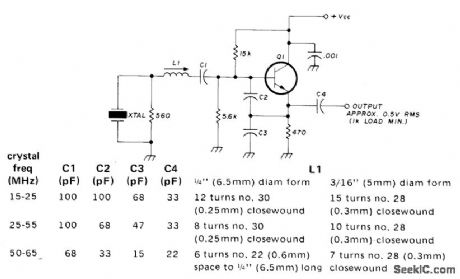
INVERTING-Uses third-overtone crystals. L1 trims crystal frequency. Resistor across crustal prevents oscillation at undesired modes. Starting is reliable and stability is good. Q1 is 2N3563, 2N3564, 2N5770, BF180, BF200, or SE1010.-R.Harrison, survey of Crystal Oscillators, Ham Radio, March 1976, p 10-22. (View)
View full Circuit Diagram | Comments | Reading(1302)
100_Hz_BANDPASS_SALLEN_KEY
Published:2009/7/2 9:25:00 Author:May
Uses one section of OP-11FY quad opamp or equivalent in circuit having Q of 4.7 and providing closed-loop gain of 200 or 46 dB. Opamp selected should have open-loop gain of 5 to 10 times required gain at resonance. Adiust resistor values to tune centerfrequency.-D. Van Dalsen, Need an Active Filter? Try These Design Aids, EDN Magazine, Nov.5, 1978, p 105-110.
(View)
View full Circuit Diagram | Comments | Reading(747)
51_55_MHz
Published:2009/7/2 9:24:00 Author:May
Tunable local oscillator is padded to tune over range required for use with 1.65-MHz IF in G.meter receiver, using Johnson type U 14-plate tuning capacitor. Can also serve as test transmitter putting out up to 20 mW. L1 is 9 tums No. 26 tapped 1 tum from low end, and L2 is 1 or 2 turns. Article covers constluction in 1 1/4 × 1 1/4 × 1/2 inch box.-B. Hoisington, A Real Hot Ftont End for Six, 73 Magazine, Nov. 1974, p 88-90 and 92-94. (View)
View full Circuit Diagram | Comments | Reading(547)
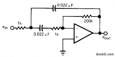
1_kHz_VARIABLE_GAIN_STATE_VARIABLE
Published:2009/7/2 9:23:00 Author:May
Damping signal is inverted with fourth opamp to make gain and damping as well as frequency independently adjustable. Damping is in range of 0-2, with critical value of 1.414 giving flattest response. For high pass, take output from first opamp; for bandpass, take output from second opamp. Value of input resistor is 10K (10,000 ohms) when gain K is 1.-D. Lancaster, Active- Filter Cookbook, Howard W. Sams, Indianapolis, IN, 1975, p 135-136. (View)
View full Circuit Diagram | Comments | Reading(618)
1_Hz_WITH_01_Hz_BANDWIDTH
Published:2009/7/2 9:22:00 Author:May

Three pots provides easy trimming to precise values desired. Use R2A to trim bandwidth to exactly 0.100 Hz, Use R1A to trim gain to exactly 10.00.Finally, trim center frequency to exactly 1.000 Hz. Ad justments are almost perfectly noninteracting if made in sequence given.-R. A.Pease, Band-Pass Active Filter with Easy Trim for Center Frequency, Teledyne Philbrick, Dedham,MA,1972, Applications Bulletin 4. (View)
View full Circuit Diagram | Comments | Reading(649)
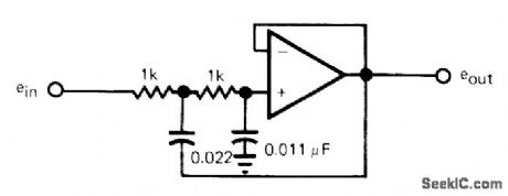
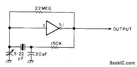
10_Hz_HIGH_PASS_UNITY_GAIN
Published:2009/7/2 9:20:00 Author:May

Low cutoff frequency is 10 Hz in active filter using opamp as voltage-controlled voltage source. Altemative opamps can be 1556 and 8007.-W.Jung, IC OpAmp Cookbook, Howard Sams, Indianapolis, IN, 1974, p 331-333. (View)
View full Circuit Diagram | Comments | Reading(510)
1_MHz_FET_PIERCE
Published:2009/7/2 9:20:00 Author:May
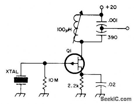
Field-effect transistor serves in place of vacuum triode in Pierce oscillator. Circuit values are for 1 MHz, but tuned circult can be adjusted to other desired frequency. Q1 can be 2N4360 or T1M12.-Circuits, 73 Magazine, March 1974, p 89. (View)
View full Circuit Diagram | Comments | Reading(660)
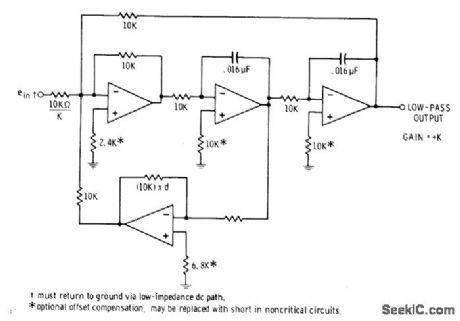
10_kHz_LOW_PASS_SALLEN_KEY
Published:2009/7/2 9:19:00 Author:May
ArticIe gives design equations from which values of components were obtained. Critical damping (Q=0.71) is provided, Frequency can be tuned over range of two decades by changing resistor values simultaneously. Opamp can be one section of OP-11FY. For equivalent high-pass filter, transpose positions of resistors and capacitors.Gain is unity.-D. Van Dalsen, Need an Active Filter? Try These Design Aids, EDN Magazine, Nov. 5, 1978, p 105-110. (View)
View full Circuit Diagram | Comments | Reading(539)
422_kHz_NOTCH
Published:2009/7/2 9:18:00 Author:May
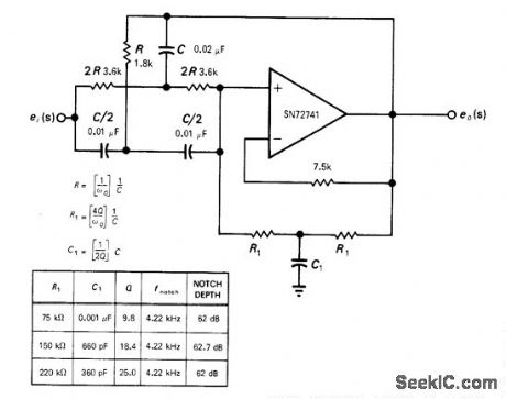
Circuit consists of positive unity-gain opamp, RC twin-T network, and T network R1C1 that determines circuit Q. Variable Q feature is controlled by single passive RC network. Center frequency of notch filter is about 4.22 kHz. Table gives values of R1 and C1 for three different values of Q.-H. T. Russell, Notch Filter Has Passive Q Control, EDN/EEE Magazine, July 1, 1971, p 43 and 45. (View)
View full Circuit Diagram | Comments | Reading(877)
PASS_REJECT_TUNABLE_NOTCH
Published:2009/7/2 9:16:00 Author:May
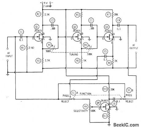
Full rotation of ganged tuning control R4 tunes circuit from 100 Hz to 10 kHz, with position of switch S1 determining whether circuit passes or rejects frequency to which it is tuned. Maximum selectivity, conesponding to maximum height of pass curve or depth of reject curve and minimum width of either curve, is obtained when R9 is set for maximum gain in FET Q4. If R9 is advanced far enough with switch set to pass, circuit will oscllate and give sine-wave output at tuned frequency.-R.P.Tumer, FET Circuits, Howard W, Sams, Indianapolis, IN, 1977, 2nd Ed., p 71-73. (View)
View full Circuit Diagram | Comments | Reading(521)
DC_LEVEL_SHIFTER_FOR_AF
Published:2009/7/2 9:13:00 Author:May

Circuit using optical Electronics 9803 opamps separates AF input signal into two outputs. Low-pass output contains DC to 10 Hz, and high-pass output has frequency content above 10 Hz to upper frequency limit approaching 10 MHz for opamp used. Dynamic output impedance of both outputs is less than 1 ohm. Both outputs have DC continuity. DC output of high-pass terminal is equal to offset voltage of integrator. DC output of low-pass terminal equals DC input plus offset voltages of both opamps.- Automatic DC Level Shifter, Optical Electronics, Tucson, AZ, Application Tip 10226. (View)
View full Circuit Diagram | Comments | Reading(941)
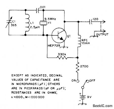
1_MHz_WITH_ONE_GATE
Published:2009/7/2 9:10:00 Author:May
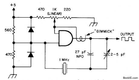
Crystal oscillator uses only onesection of SN7408 TTL quad AND gate. Use series-resonant crystal having 30-pF series capacitance. Adjust 1K pot for reliable start-up and symmetrical square-wave output. Diodes are 1N34A or 1N914. Gimmick is 1 or 2 turns of insulated wire wrapped around output lead.-Clyde E. Wade, Jr., An Even Simpler Clock Oscillator, 73 Magazine, Nov./Dec. 1975, p 164. (View)
View full Circuit Diagram | Comments | Reading(716)
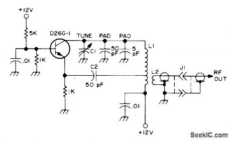
LOW_NOISE_5_MHz
Published:2009/7/2 9:09:00 Author:May
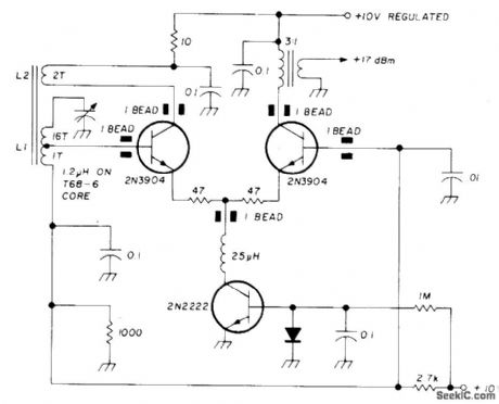
Very low-noise high-QLC oscillator operating at 5 MHz is designed for use in high-performance communication receivers. Oscillator uses two stages, one oporating in class A and the other operating as limiter that also serves as feedback path.-U. L. Rohde, Effects of Noise in Receiving Systems, Ham Radio, Nov. 1977, p 34-41. (View)
View full Circuit Diagram | Comments | Reading(537)
CRYSTAL_WITH_CMOS_INVERTER
Published:2009/7/2 9:09:00 Author:May
Simple mono multivibrator circuit using MC14007 or CD4007 operates in frequency range from 10 kHz up to top limit of about 10MHz, with exact frequency depending on values used for R and C. Pin 7 of IC is VSS and pin 14 is VDD. Pins 5 and 1 must be connected together for proper operation.-W. J. Prudhomme, CMOS Oscillators, 73 Magazine, July 1977, p 60-63. (View)
View full Circuit Diagram | Comments | Reading(950)
50_kHz_MEACHAM_BRIDGE
Published:2009/7/2 9:07:00 Author:May
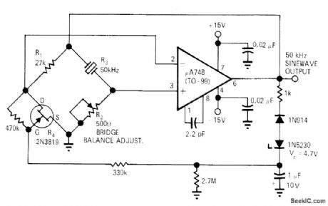
Crystal osyillator using Meacham bridge requires no transformers for producing low-distortion sine-wave output. Quartz crystal should be cut for operation in series-resonant mode. With minor modifications, same circuit can be used for 100- and 200-kHz crystals. By adding single-transistor stage, oscillator can be used as clock generator for TTL circuits.-K. J. Peter, Stable Low-Distortion Bridge Oscillator, EDN|EEE Magazine, Nov. 15, 1971, p 50-51. (View)
View full Circuit Diagram | Comments | Reading(1452)
100_kHz_CRYSTAL_DIODE_RELAXATION
Published:2009/7/2 9:00:00 Author:May
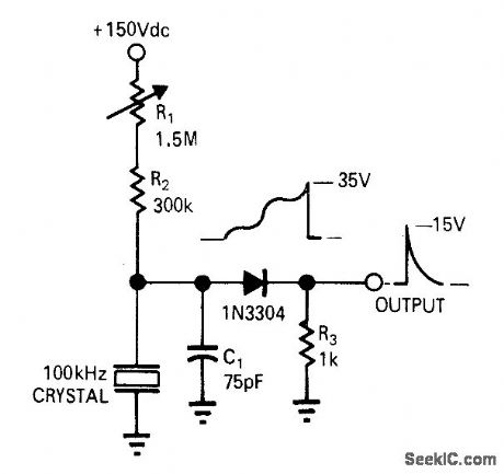
Crys tal-controlled relaxation oscillator uses 1N3304 four-layer diode as active element, R1 adjusts RC time constantso oscillator locks at fundamental frequency of crystal or at half this frequency.-R. D. Clement and R. L. Starliper, Crystal-Controlled Relaxation Oscillator, EDN|EEE Magazine, Oct. 15, 1971, p 62 and 64. (View)
View full Circuit Diagram | Comments | Reading(871)
INCREASING_CRYSTAL_FREOUENCY
Published:2009/7/2 8:59:00 Author:May
Adding parallel resonant circuit across crystal, tuned slightly above crystal frequency, makes oscillator frequency increase. Some plated crystals will work better than others in this circuit; third-overtone types operating on their fundamental generally give best results. Article covers theory of operation.-L. Lisle, The Tunable Crystal Oscillator, QST, Oct. 1973, p 30-32. (View)
View full Circuit Diagram | Comments | Reading(902)
50_Hz_WIEN_BRIDGE_NOTCH_FILTER
Published:2009/7/2 8:52:00 Author:May

Uses opamp in circuit having essentially zero output impedance, making additional buffer amplifier unnecessary. Article gives design theory and covers many other types of notch filters.-Y.Nezer, Active Notch Filters, Wireless World, July 1975, p 307-311. (View)
View full Circuit Diagram | Comments | Reading(1713)
FREQUENCY_TRACKING_BANDPASS
Published:2009/7/2 8:49:00 Author:May

High-Q active bandpass filter automatically tracks input signal frequency over 10:1 range in presence of noise.When signal goes outside tracking range, circuit sweeps between low- and high-frequency limits until suitable signal reappears. Circuit is basically voltage-controlled bandpass filter using Optical Electronics 3704 active filter with 5898 analog multipliers. 9813 opamp connected as Schmitt trigger is main element of scanning circuit. Frequency range is 160 to 1600 Hz, and FM bandwidth of error-voltage output is 20 Hz.- Frequency Tracking Active Filter, Optical Electronics, Tucson, AZ, Application Tip 10270. (View)
View full Circuit Diagram | Comments | Reading(1060)
1_kHz_MULTIPLE_FEEDBACK_BANDPASS
Published:2009/7/2 8:47:00 Author:May

Single 741 or equivalent opamp is suitable for applications where bandwidth is less than 100%.Gain is fixed at -2Q2, where Q is reciprocal of damping d and ranges from less than 1 to above 100. Q is changed by varying ratio of input and feedback resistors while keeping their product constant. For Q of 3, feedback resistor should be 36 times value of input resistor.-D. Lancaster, Active-Filter Cookbook, Howard W. Sams, Indianapolis, IN, 1975, p 150-154. (View)
View full Circuit Diagram | Comments | Reading(817)
| Pages:288/471 At 20281282283284285286287288289290291292293294295296297298299300Under 20 |
Circuit Categories
power supply circuit
Amplifier Circuit
Basic Circuit
LED and Light Circuit
Sensor Circuit
Signal Processing
Electrical Equipment Circuit
Control Circuit
Remote Control Circuit
A/D-D/A Converter Circuit
Audio Circuit
Measuring and Test Circuit
Communication Circuit
Computer-Related Circuit
555 Circuit
Automotive Circuit
Repairing Circuit