
Basic Circuit
Index 292
VARIABLE_HYSTERESlS_SCHMITT
Published:2009/7/2 4:18:00 Author:May
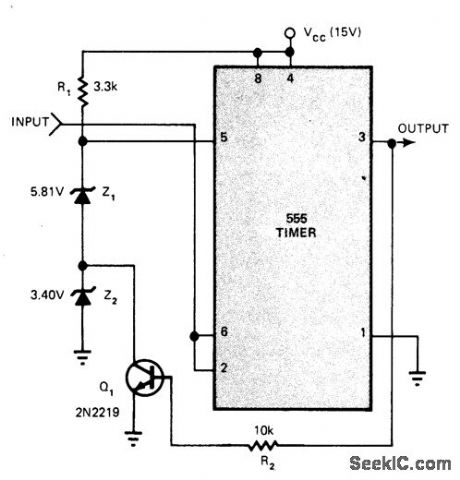
Uses standard 555 timer with only five additional components to give fully TTL/DTL-compatible Schmitt trigger that responds to slow input ramps as well as straight DC levels. When input is 0, output goes high and tums on Q1. When input increases to 5.8 V, output goes low and Q1, tums off. Decreasing output to 4.7 V (lower threshold point) makes output high again. For values shown, hysteresis is thus 1.1 V. Threshold points and hysteresis value can be adjusted as required by changing zeners used.-M. K.Lalitha and P. R. Chetty, Variable-Threshold Schmitt Trigger Uses 555 Timer, EDN Magazine, Sept. 20, 1976, p 112 and 114. (View)
View full Circuit Diagram | Comments | Reading(570)
ELECTRONIC_CROSSOVER_CIRCUIT
Published:2009/7/2 4:18:00 Author:May
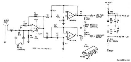
An audio source, such as a mixer, preamplifier, equalizer, or recorder, is fed to the Electronic Crossover Circuit's input. That signal is either ac- or dc-coupled, depending on the setting of switch 51, to the non-inverting input of buffer-amplifter U1a, one section of a quad, BIFET, low-noise TL074 op amp made by Texas Instruments. That stage has a gain of 2, and its output is distributed to both a lowpass filter made by R4, R5, C2, C3, and op-amp Uld, and a highpass filter made by R6, R7, C4, C5, and op amp Ulc. Those are 12 dB/octave Butterworth-type filters. The Butterworth filter response was chosen because it gives the best compromise between damping and phase shift. Values of capacitors and resistors will vary with the selected crossover at which your unit will operate. The filter's outputs are fed to a balancing network made by R8, R9, R10, R11 and balance potentiometer R14. When the potentiometer is at its mid-position, there is unity gain for the passbands of both the high and low filters. Dc power for the Electronic Crossover Circuit is regulated by R12, R13, D1, and D2, and decoupled by C6 and C7. (View)
View full Circuit Diagram | Comments | Reading(3798)
LOW_PASS_DIGITAL_FILTER
Published:2009/7/2 4:15:00 Author:May

Used to retrieve pulse train data from noisy signal line. Filtering is achieved with SN7400 quad two-input NAND gate, SN7413 dual four-input Schmitt trigger, two diodes, and two capacitors. One gate of SN7400 is used as inverter driving pulse delay operating on negative-going transition of input pignal. Other Schmitt trigger, diode, and capacitor provide delay on positive-going transition. Any additional pulses occurring during delaycirouit time-out resets delay time without affecting output.-T. H. Haydon. Low-Pass Digital Filter. EDN Magazine. Nov. 20. 1973. p 85. (View)
View full Circuit Diagram | Comments | Reading(1701)
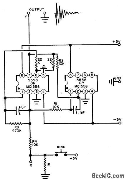
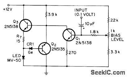
SLIDING_TONE_DOORBELL
Published:2009/7/2 4:14:00 Author:May
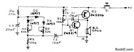
When the doorbell is pushed, you'll hear a low tone that will slide up to a higher frequency. The frequency of the AF oscillator is determined by coupling capacitor, C1 and the value of the resistance connected between the base of Q1 and ground. That resistance, RBG is equal to (R1 + R2) R3. First, assume that 51 is closed and R2 has been adjusted td produce a pleasant, low-frequency tone. Capacitor C3 will charge through R6 until it reaches such a voltage that it will cause diode D1 to conduct. When that happens, the value of RBG is paralleled by R4, Thus, because the total resistance RBG decrease, the output tone slides up in frequency. Capacitor C3 will continue to charge until the voltage across D2 and D3 causes those diodes to conduct. Then RBG is paralleled also by R5, the total resistance again decreases, and the oscillator's frequency again increases. (View)
View full Circuit Diagram | Comments | Reading(503)
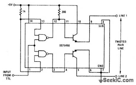
BALANCED_LINE_DRlVER
Published:2009/7/2 4:13:00 Author:May

National DS75450 dual peripheral driver serves as interface between TTL and twisted-pair line. Output line 1 is terminated to ground through haff of line impedance, and line 2 is terminated to +5 V through half of line impedance. Output current is 300 mA.- Interface Databook, National Semiconductor, Santa Clara, CA, 1978, p 3-20-3-30. (View)
View full Circuit Diagram | Comments | Reading(509)
ELECTRONIC_BELL
Published:2009/7/2 4:12:00 Author:May
Coarse frequency is controlled by the capacitors which must be kept nearly identical in value to each other for best results. Fine tuning is accomplished with R1 and R2. The decay time is controlled by R3. (View)
View full Circuit Diagram | Comments | Reading(1127)
LOU_COST_CHIME_CIRCUIT
Published:2009/7/2 4:11:00 Author:May
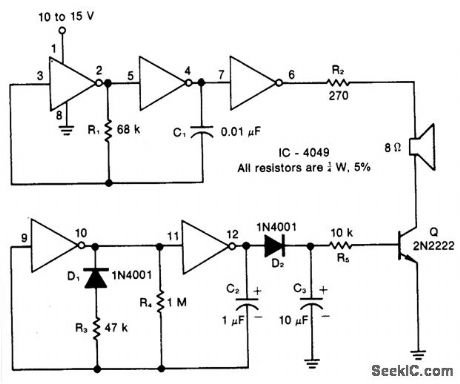
Resistor R1, capacitor C1, and two inverters form a square wave generator, which produces the basic tone. The generator is followed by an inverter that acts as both a buffer and a driver for the speaker. Resistor R2, which has a minimum value of 100 ohms, limits the current and controls the volume. Diode D1, ca-pacitor C2, resistors R3 and R4, and two inverters create the pulse generator that determines the turn-on and decay times of the chime. The decay circuit-formed by D2, C3, R5, and Q-reduces the amplitude of the chime tone exponentially as a function of time. (View)
View full Circuit Diagram | Comments | Reading(585)
CMOS_INTERFACE_FOR_OPAMP
Published:2009/7/2 4:08:00 Author:May
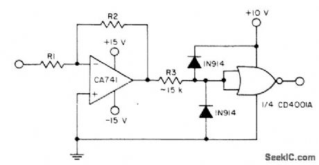
Clamp diodes and single resistor provide interface between CMOS circuit and opamp operating between normal ±15 V supply rails. Diodes ensure that CMOS input voltage does not go outside permissible range.- COS/MOS Integrated Circults, RCA Solid State Division,Somerville,NJ,1977,p 629 (View)
View full Circuit Diagram | Comments | Reading(464)
AND_LOGIC_FOR_MUTlNG
Published:2009/7/2 3:53:00 Author:May
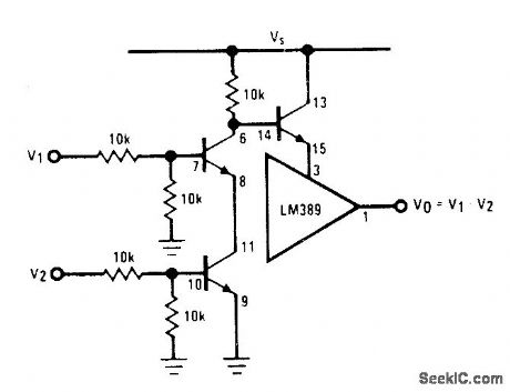
Connection shown for National LM389 combination of three transistors with opamp gives standard AND circuit for controlling muting transistor in audio sys tem. Shorting pin 12 of opamp to ground gives NAND Iogic.- Audio Handbook, National Semiconductor, Santa Clara, CA, 1977, p 4-33-4-37. (View)
View full Circuit Diagram | Comments | Reading(607)
LATCH
Published:2009/7/2 3:51:00 Author:May
National LM3909 IC operating from 3-V battery requires only momentary contact by switch to change logic level of output and hold that level.- Linear Applications.Vol, 2, National Semiconductor, Santa Clara,CA,1976,AN-154,p9 (View)
View full Circuit Diagram | Comments | Reading(606)
500_kHz_SWITCHING_INVERTER_FOR_12_V_SYSTEMS
Published:2009/7/2 3:48:00 Author:May

Circuit Notes
This PWM control circuit provides the control pulse to the DMOS Power Switch in the flyback circuit. The output of the PWM is a pulse whose width is proportional to the input control voltage and whose repetition rate is determined by an external clock signal. To provide the control input to the PWM and to prevent the output voltage from soaring or sagging as the load changes the error amplifier and reference voltage complete the design. They act as the feedback loop in this control circuit much like that of a servo control system. (View)
View full Circuit Diagram | Comments | Reading(505)
INTERFACE_FOR_INDUSIRIAL_CONTROL
Published:2009/7/2 3:47:00 Author:May
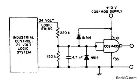
Simple resistive divider circuit provides interfacebetween 24-V logic swing of industrial controlsystem and CMOS logic operating from 10-Vsupply Filter capacitor enhances excellentnoise immunity of CMOS logic Clamp diodesensure thatinput signal voltage is between VDD and Vss-″cos/MOS Integrated Circuits'″RCA Solid State Division, Somerville, NJ, 1977, p628. (View)
View full Circuit Diagram | Comments | Reading(414)
TTY_LINK_FOR_MICROPROCESSOR
Published:2009/7/2 3:43:00 Author:May
Demonstration circuit illustrates use of fiber-optic cable with low-cost components for relatively narrow-band application, to provide feed from remote teleprinter to microprocesson.-O. E.Marvel and J. C. Freeborn, A Little Hands-On Experience llluminates Fiber-Optic Links, EDN Magazine,Nov.5,1977,p 71-75. (View)
View full Circuit Diagram | Comments | Reading(488)
1_MHz_LED_PULSE_MODULATION
Published:2009/7/2 3:40:00 Author:May
Circuit provides required low driving-point impedance for fast turn-on of gallium arsenide phosphide LED used as source for high-speed pulse modulation of fiber-optic or otherlight beam. Q1 supplies DC level and modulation information to emitterfollower output stage Q3. Output current is sensed and limited to about 30 mA by Q2. Turn-on time for full brightness is 12 ns.-G.Schmidt, LED Modulator, EDN/EEE Magazine, June 15,1971,p 57. (View)
View full Circuit Diagram | Comments | Reading(482)
SEWING_MACHINE_SUPPRESSION
Published:2009/7/2 3:30:00 Author:May
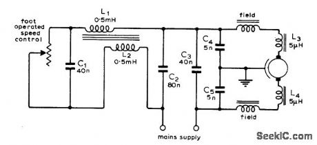
Circuit is used to suppress clicks from speed control aswell as intelf erence produced by motor itselfinsound and television broadcast bands.-A s McLachlan J .H .Ainley and R.J Harry. Radio Interfererce-a Review Wireless World. June1974.p 191-195. (View)
View full Circuit Diagram | Comments | Reading(496)
ALARM_DRIVES_PAGING_BEEPER
Published:2009/7/2 3:24:00 Author:May
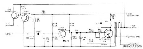
Complete protection of vehicle is provided by multiplicity of door-switch, mat-switch, vibration, motion, and other sensors connected to common sen-sor input of alarm switching circuitthat controls radio pager, 1-W GE Voice Command II trans-mitter operating around 147 MHz, 100-W electronic siren, and power horns. Closing of con tacts in any sensor grounds common input (assuming keylock switch has been closed to arm circuit by applying +12 V), applying power to siren and pager system. Range is about 1 mi for Motorola Pageboy II cigarette-pack-size pager receiver. Article describes construction, operation, and installation in detail and gives complete circuit of pager.-J. Crawford, Build a Beeper Alarm, 73 Magazine, Oct. 1977, p 68-77.
(View)
View full Circuit Diagram | Comments | Reading(842)
MULTIPLE_FEEDBACK_BANDPASS_FILTER
Published:2009/7/2 3:22:00 Author:May


The op amp is connected in the inverting mode. Resistor R3 from the output to the inverting input sets the gain and current through the frequency-determining capacitor, C1. Capacitor C2 provides feedback from the output to the junction of R1 and R2.C1 and C2 are always equal in value. Resistor R2 may be made adjustable in order to adjust the center frequency which is determined from:When designing a filter of this type it is best to select a value for C1 and C2, keeping them equal. Typical audio filters have capacitor values from 0.01,μF to 0.1,μF which will result in reasonable values for the resistors. (View)
View full Circuit Diagram | Comments | Reading(0)
BANDPASS_AND_NOTCH_FILTER
Published:2009/7/2 3:19:00 Author:May

The Quad op amp MC4301 is used to configure a ftlter that will notch out a given frequency and produce that notched-out frequency at the BP terminal, useful in communications or measurement setups. By proper component selection any frequency ftlter up to a few tens of kilohertz can be obtained. (View)
View full Circuit Diagram | Comments | Reading(797)
7_SEGMENT_TO_BCD
Published:2009/7/2 3:17:00 Author:May
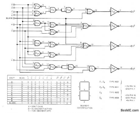
Uses six CMOS packages to convert 7-segment display to corresponding four-line positive-logic BCD code for digits 0-9. Added feature is blank input which, when high,foroes blank code(1110 or 1111)into readout,for use in suppressing leading zeros with some types of data storage.Use 4010 in place of 4009 for Z6 when negative-logic BCD output is required.—R. Sturla, Real-Time 7-Seg-ment to BCD Converter, EDN Magazine, June 20, 1973, p 89. (View)
View full Circuit Diagram | Comments | Reading(7825)
ACTIVE_BANDPASS_FILTER
Published:2009/7/2 3:16:00 Author:May


The circuit is a two-pole active filter using a TL081 op amp. This type of circuit is usable only for Qs less than 10. The component values for this filter are calculated front the following equations.The values shown are for a center frequencyof 800 Hz. (View)
View full Circuit Diagram | Comments | Reading(1457)
| Pages:292/471 At 20281282283284285286287288289290291292293294295296297298299300Under 20 |
Circuit Categories
power supply circuit
Amplifier Circuit
Basic Circuit
LED and Light Circuit
Sensor Circuit
Signal Processing
Electrical Equipment Circuit
Control Circuit
Remote Control Circuit
A/D-D/A Converter Circuit
Audio Circuit
Measuring and Test Circuit
Communication Circuit
Computer-Related Circuit
555 Circuit
Automotive Circuit
Repairing Circuit