
Basic Circuit
Index 298
ALARM_FOR_SPECTRUM_ANALYZER
Published:2009/7/1 21:21:00 Author:May

Circuit drives audible alarm when frequency of interest appears in spectrum range. Display cursor can be preset to initiate narrow search band in which fx is expected to appear. 100-μs pulse representing cursor position in display sweep triggers mono IC1 so its output becomes window whose time-out is equivalent to band in which fx is center. Comparator A1 supplies high output when fx appears. Simultaneous arrival of this signal and timer window at gate A sets output of left flip-flop high. At end of window period, right flip-flop also goes high and initiates alarm via Q1. Loss of fX stops alarm.-R. L. Messick, Alarm Simplifies Spectrum-Analyzer Measurements, EDN Magazine, JuneS, 1978, p 152. (View)
View full Circuit Diagram | Comments | Reading(698)
5_DIGIT_LED_REAL_TIME
Published:2009/7/1 21:20:00 Author:May
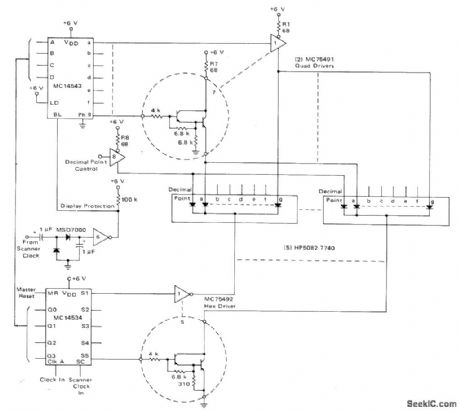
Circuit providesstrobing of LEDs so peak current and light output are greater for same average current Peak fotward current for display is about 40 mA. All Iike anode segments of common-cathode displays are driven by emitter outputs of MC75491 quad drivers.-A. Pshaenich, Interface Considerations for Numeric Display Systems, Motorola, Phoenix, AZ, 1975, AN-741, p 13. (View)
View full Circuit Diagram | Comments | Reading(608)
5_MHz_PHASE_ENCODED_DATA_READ_CIRCUITRY
Published:2009/7/1 21:18:00 Author:May
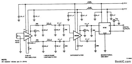
Readback data is applied directly to the input of the first NE592. This amplifier functions as a wide-band ac coupled amplifier with a gain of 100. By direct coupling of the readback head to the amplifier, no matched terminating resistors are required and the excellent common-mode rejection ratio of the amplifier is preserved. The dc components are also rejected because the NE592 has no gain at dc due to the capacitance across the gain select terminals. The output of the first stage amplifier is routed to a linear phase shift low-pass filter, with a characteristic impedance of 200 ohms. The second NE592 is utilized as a low noise differentiator/amplifier stage. The output of the differentiator/amplifier is connected to the 8720 bidirectional monostable unit to provide the proper pulses at the zero-crossing points of the differentiator. (View)
View full Circuit Diagram | Comments | Reading(563)
V_F_CONVERSION,NEGATIVE_INPUT_VOLTAGE
Published:2009/7/1 21:18:00 Author:May

View full Circuit Diagram | Comments | Reading(473)
327_Hz_HIGH_PASS
Published:2009/7/1 21:17:00 Author:May

Developed to make third harmonic of 130.81 Hz (C3 note) minimum of 30 dB stronger than fundamental, to give sawtooth output for use in electronic music system. Design uses third-order filter with 3-dB dips in response. Opamp can be 741.-D. Lancaster, Active-Filter Cookbook, Howard W. Sams, Indianapolis, IN. 1975. p 192. (View)
View full Circuit Diagram | Comments | Reading(532)
AUTO_ADVANCE_PROJECTOR
Published:2009/7/1 21:17:00 Author:May
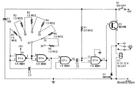
Circuit Notes
The circuit is built around a 4001 quad two-input N0R gate, it provides switch selectable auto-advance times of 5,10, 15, 20, 25 or 30 seconds through the remote-control socket of your projector. U1a and U1b form an astable multivibrator, with its operating frequency dependent on the number of timing resistors switched into the circuit via S2. The frequency is about one cycle for every five seconds with a single timing resistor, one every ten seconds with two resistors, etc., providing six switched time intervals. The output of the astable at pin 4 of U1b is fed to the input of a monostable multiibrator, consisting of the second pair of gates, U1c and U1d. R7 and C3 are the timing components; they set the length of the (positive) output pulse of the monostable at a little more than half a second. The monostable is triggered by each positive-going input it receives from the astable. The output from the monostable therefore, consists of a series of short pulses, the interval between the pulses being controlled using S2.The output of the monostable (at pin 11) controls a relay by way of Q1, which is configured as an emitter-follower buffer stage. The projector is controlled via the normally-open contacts of relay K1. When the output of the monostable goes positive, the relay contacts close, triggering the slide-change mechanism of the projector. The monostable assures that the power to the relay is applied only briefly by the timer, so that multiple operation of the projector is avoided. (View)
View full Circuit Diagram | Comments | Reading(1196)
DIFFERENTIAL_HOLD
Published:2009/7/1 21:17:00 Author:May
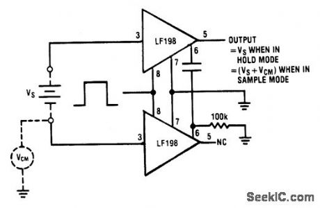
View full Circuit Diagram | Comments | Reading(0)
TWO_WIRE_TONE_ENCODER
Published:2009/7/1 21:16:00 Author:May
View full Circuit Diagram | Comments | Reading(535)
GUITAR_AND_BASS_TUNER
Published:2009/7/1 21:14:00 Author:May
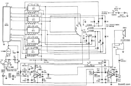
The heart of the circuit is IC2, a 50240 top-octave generator. That device uses a single input-frequency to generate all twelve notes of the musical scale. The input signal is provided by IC1, a 4001 quad 2-input NOR gate. Two sections of that IC are used to form an oscillator that runs at approximately 2 MHz. The frequency can be adjusted by trimmer potentiometer R2. Dual D flip-flops, IC3-IC7, are used as frequency dividers. They divide down the upper-octave frequencies from IC2, thus generating the lower-frequency notes required for the pitch references. The chords for the bass pitchreferences are composed of three notes each. Those notes are taken from various outputs of IC2-IC7 through isolation diodes D1-D12. A1 signals are routed to the TONE switch, S3. The wiper arm of that switch is connected through R7 to the input of audio power-amplifier IC8, an LM386. The resistor acts as a volume control for the pitch reference.Another LM386, IC9, serves as an amplifier for the instrument being tuned, with R10 acting as its volume control. The outputs of IC8 and IC9 are coupled, through C5 and C12 respectively, to the headphone jack, J1. Switch S2 STEREO/MONO is used to mix the reference and instrument signals at IC9 for mono operation. Power is supplied by eight AA cells connected in series. (View)
View full Circuit Diagram | Comments | Reading(1652)
MULTIPLEXING_EIGHT_DlGITS
Published:2009/7/1 21:14:00 Author:May
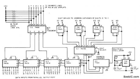
Uses only one 7-segment driver for eight digits of parallel BCD data on eight-LED display that can use MAN 4 or DL7647-segment LEDs. Power is supplied to only one digit at a time but is switched at high enough rate so all digits appear to be on. Uses one eight-channel 74151 multiplexerfor each of the 4 data input bits. Multiplexors and demultiplexer are addressed by7493 counter that is incremented at about 4 kHz by 555 oscillator.IC11 is connected for three-to eight-line demultiplexing. IC7-IC10 are peripheral interface gates, each sinking up to 300 mA for its LED.7448 decoder/driver converts BCD data to 7-segment code for driving segments of LEDs. For 74151 and 74155, pin 16 goes to +5 V and pin 8 to ground. Pin 8 of 75451 goes to +5 V and pin 4 to ground. Pin 5 of 7493 goes to +5 V and pin 10 to ground.-J. Hogenson, Multiplex Your Digital LED Displays, BYTE, March 1977, p 122-126 and 128. (View)
View full Circuit Diagram | Comments | Reading(2574)
V_F_CONVERSION_POSITIVE_INPUT_VOLTAGE
Published:2009/7/1 21:13:00 Author:May
View full Circuit Diagram | Comments | Reading(853)
10_kHz_LOW_PASS_FILTER
Published:2009/7/1 21:13:00 Author:May

Suitable for use at both input and output of A/D-D/A converter in digital audio system for synthesizing speech or music. Serves for smoothing steps of output waveform and suppressing background noise on output when small signals are being processed with 8-bit Iinear encoding.-T. Scott. Digital Audio. Kilobaud, May 1977. p 82-86. (View)
View full Circuit Diagram | Comments | Reading(844)
PULSE_AND_SEQUENCE_OUTPUTS
Published:2009/7/1 21:09:00 Author:May

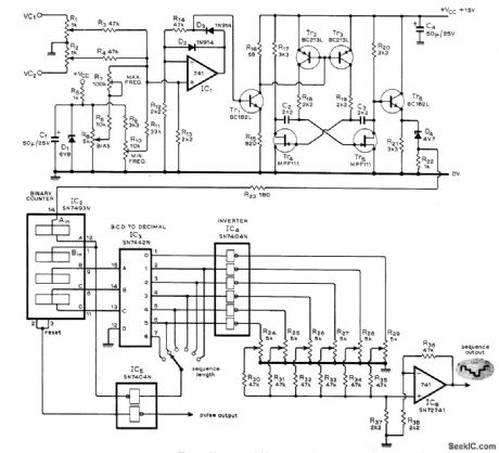
Voltagecontrolled oscillator produces sequence of steps, with amplitude of each step individually controllable up to maximum of six steps. Circuit also generates series of pulses having 1 : 1 markspace ratio. each coincident with leading edge of a step. Pair of summing inputs controls oscillator, with exponential frequency-voltage relationship extending in one range from subsonic frequencies to over 20 kHz. Used in sound synthesizer described in three-part article that gives all circuits and operating details. Applications include synthesizing sounds ranging from bird distress calls and engine noises to spoken words and wide variety of musical Instruments.-T. Orr and D W,Thomas、 Electronic Sound Synthesizer、Wireless World, Part2-Sept 1973.p 429-434 (Part 1-Aug,1973.p366-372; Part 30-ct 1973.p485-490). (View)
View full Circuit Diagram | Comments | Reading(916)
INEXPENSIVE_RADIO_CONTROL_USES_ONLY_ONE_SCR
Published:2009/7/1 21:08:00 Author:May
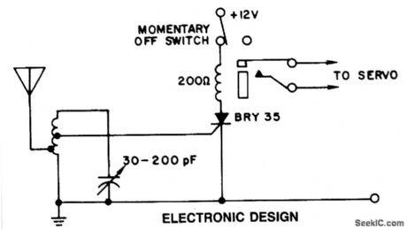
A simple and effective receiver for actuating garage doors, alarms, warning systems, etc.The SCR, which has a very low trigger current 30μA is typical-it requires an input power of only 30μW to activate the relay. A high Q tuned antenna circuit assures rejection of spurious signals. A whip or wire antenna is adequate up to 100 feet from a low power transistor transmitter. A momentary-off switch resets the circuit. (View)
View full Circuit Diagram | Comments | Reading(719)
SINGLE_LED_CAN_INDICATE_FOUR_LOGIC_STATES
Published:2009/7/1 21:07:00 Author:May
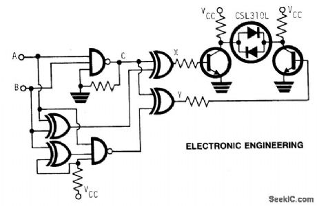
The LED is the CSL310L which contains a red LED and a green LED connected back to back and mounted close together in a single moulding. The LED can emit red or green light by controlling the polarity of the applied voltage and if the polarity is switched at a rate of several hundred Hertz the emitted light appears yellow. The four combinations of inputs A and B can therefore be converted to four LED states-red, green, yellow and off. The truth table shows the LED colors corresponding to the combinations of A and B levels.
Truth TableA B X Y LED Color1 0 0 1 0 red0 1 0 0 off1 0 0 1 green1 1 C C yellow
(View)
View full Circuit Diagram | Comments | Reading(550)
MUSICAL_BELLS
Published:2009/7/1 20:57:00 Author:May

Opamp connected as active filter simulates attack followed by gradual decay as produced when bell or tuning fork is struck. Filter portion of circuit uses twin-T network adjusted so active filter breaks into oscillation when slight external disturbance is intro-duced by closing S1 momentarily. Circuit feeds external audio amplifier and loudspeaker for converting ringing frequency into audible sound. Set R3 just below oscillation point. R1and R2 can be adjusted to give sounds of other musical instruments, such as drums, bamboo, and triangles.-F. M. Mims, Electronic Music Projects, Vol. 1, Radio Shack, Fort Worth, TX, 1977, 2nd Ed., p 71-80. (View)
View full Circuit Diagram | Comments | Reading(1355)
MODEL_ROCKET_LAUNCHER
Published:2009/7/1 20:56:00 Author:May
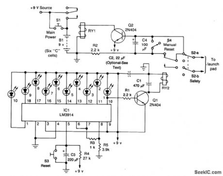
The circuit consists of the launch timer itself and an automatic-off timer. When power is applied to that IC, the countdown LED's sequence is on until they are all lit. When the last one LED1, is fully lit, transistor Q1 saturates, energizing RY2. When that happens, a circuit between the lantern battery at the launch pad and the nickel-chromium wire is completed; the wire heats up as before, and the rocket is launched. Resistor R4 and capacitor C3 determine the countdown timing; with the values shown it should be approximately 10 seconds. Resistors R3 and R5 set the LED brightness. Safety is of the utmost importance. That's the purpose of the second half of the circuit. When RY2 opens, the current flow to Q2 is disrupted. But, because of the presence of R2 and C4, the transistor remains saturated for about 3 seconds. After that, however, the transistor stops conducting and RY1 is de-energized. That cuts off the power to the rest of the circuit, and RY2 de-energizes again, breaking the circuit to the launch pad. Switch S3 is used to reset the countdown. Once that is done, pressing S1 starts the launch sequence; the rest is automatic. Switch S4 is used to latch RY1 manually if needed. (View)
View full Circuit Diagram | Comments | Reading(1200)
6_DIGIT_FLUORESCENT_TRIODES
Published:2009/7/1 20:56:00 Author:May
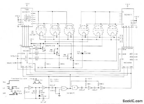
Uses two sets of cascaded counters and decoders with series switching of positive voltage to anode with MC14511 ICs. Digit scanning is accomplished by turning on grid control transistors Q1-Q3 with negative-going digit select outputs of one MC14553, Timing for counters is derived from MC14572 logic elements, with disable pulse obtained from two astable MVBRs. Display digits can be packaged individually or in single envelope.-A. Pshaenich, Interface Considerations for Numeric Display Systems, Motorola, Phoenix, AZ, 1975, AN-741, p 9. (View)
View full Circuit Diagram | Comments | Reading(1045)
SQUIB_FIRING_CIRCUIT_Ⅱ
Published:2009/7/1 20:54:00 Author:May
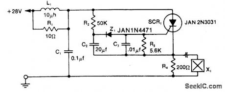
The LRC input network limits the anode dvidt to a safe value-below 30V/μs. R1 provides critical damping to prevent voltage overshoot. While a simple RC filter section could be used, the high current required by the squib would dictate a small value of resistance and a much larger capacitor. Resistor R3 provides dc bias stabilization, while C3 provides stiff gate bias during the transient interval when anode voltage is applied.The SCR is fired one second after arming by means of the simple R2C2Z1 time delay network. R4 provides a load for the SCR for testing the circuit with the squib disconnected-limiting the current to a level well within the continuous rating of the SCR.The circuit can be reset by opening the +28 V supply and then re-arming. (View)
View full Circuit Diagram | Comments | Reading(647)
SQUIB_FIRING_CIRCUIT_Ⅰ
Published:2009/7/1 20:53:00 Author:May
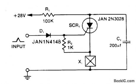
Capacitor C1 is charged to + 28V through R1 and stores energy for firing the squib. A positive pulse of 1mA applied to the gate of SCR1 will cause it to conduct, discharging C1 into the squib load X1. With the load in the cathode circuit, the cathode rises immediately to +28 V as soon as the SCR is triggered on.Diode D1 decouples the gate from the gate trigger source, allowing the gate to rise in potential along with the cathode so that the negative gate-to-cathode voltage rating is not exceeded. This circuit will reset itself after test firing, since the available current through RI is less than the holding current of the SCR. After C1 has been discharged, the SCR automatically turns off-allowing C1 to recharge. (View)
View full Circuit Diagram | Comments | Reading(685)
| Pages:298/471 At 20281282283284285286287288289290291292293294295296297298299300Under 20 |
Circuit Categories
power supply circuit
Amplifier Circuit
Basic Circuit
LED and Light Circuit
Sensor Circuit
Signal Processing
Electrical Equipment Circuit
Control Circuit
Remote Control Circuit
A/D-D/A Converter Circuit
Audio Circuit
Measuring and Test Circuit
Communication Circuit
Computer-Related Circuit
555 Circuit
Automotive Circuit
Repairing Circuit