
Basic Circuit
Index 287
1_kHz_BANDPASS
Published:2009/7/2 21:11:00 Author:May

Simple circuit using voltage-fonower opamp provbides bandpass of 1 kHz centered on 1 kHz,to give outputrange of 500-1500 Hz.- The Linear and Interface Circuits Data Book for Design Engineers, Texas Instruments, Dallas, TX, 1973, p 4-39. (View)
View full Circuit Diagram | Comments | Reading(678)
14_kHz_TWIN_T_BANDPASS
Published:2009/7/2 21:08:00 Author:May

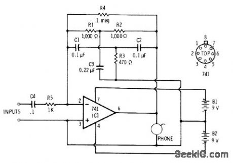
Combination of passive twin-T bandpass filter and 741 opamp gives simple audio filter for amplifying narrow frequency band (about 300 Hz wide) centered on 1.4 kHz. Filter ean be tuned to other frequencies by replacing R1 and R2 with 10K pots. Frequency is equal to 1/6.28RC where R is value in ohms of R1 and R2 and C is capadtance in farads of C1 and C2. R3 is half of R1.-F. M. Mims, Integrated Circuit Projects, Vol. 2, Radio Shack, Fort Worth, TX, 1977, 2nd Ed., p 71-80.
(View)
View full Circuit Diagram | Comments | Reading(1166)
AF_NOTCH
Published:2009/7/2 21:07:00 Author:May
Notch frequency is easily tuned at frequencies below 1 kHz with single capacitor C1 or by replacing R1 and R2 with 249K pot. For higher frequencies, use 118 opamp for A1 and 5K for R3 while lowering other resistances in proportion to R3.Indicated resistance tolerances are necessary for optimum notch depth.-W. G. Jung, IC Op-Amp Cookbook, Howard W.Sams,Indianapolis, IN, 1974, p 340-341. (View)
View full Circuit Diagram | Comments | Reading(579)
CMOS_INTERFACE_FOR_VMOS
Published:2009/7/2 21:03:00 Author:May
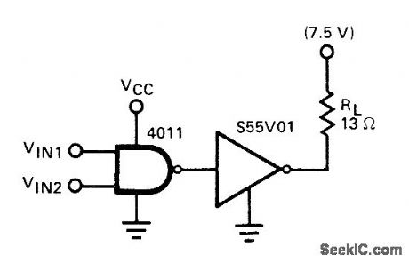
Simple 4011 CMOS gate connection provides required logic interface for S55V01 VMOS that is capable of handling up to 1 A. Switching time is about 25 ns but can be doubled by connecting four CMOS gates in parallel. Vcc can be either 10 or 15V.-L. Shaeffer, VMOS Peripheral Drivers Solve High Power Load Interface Problems, Computer Design, Dee. 1977, p 90, 94, and 96-98. (View)
View full Circuit Diagram | Comments | Reading(456)
FET_VOLTMETER
Published:2009/7/2 20:56:00 Author:May

This FETVM replaces the function of the VTVM while at the same time ridding the in-strument of the usual line cord. In addition, drift rates are far superior to vacuum tube circuits allowing a 0.5 volt full scale range which is impractical with most vacuum tubes. The low-leakage, low-noise 2N4340 is an ideal device for this application. (View)
View full Circuit Diagram | Comments | Reading(2476)
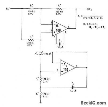
DVM_AUTO_CALIBRATE_CIRCUIT
Published:2009/7/2 20:54:00 Author:May
View full Circuit Diagram | Comments | Reading(551)
NEGATIVE_R
Published:2009/7/2 20:51:00 Author:May
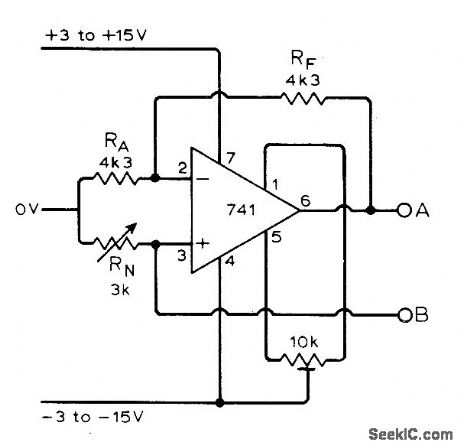
Negative-resistance connection of 741 opamp is suhable for both AC and DC applications. Requires floating power supply because 0-V terminal floats with respect to both output terminals. For DC use, adjust 10K pot to cancel offset voltage of amplifier. Value of negative resistance is varied with RN or by adjusting ratio of RF to RA. Can be used to make LC circuits operate at subaudio frequencies.-D. A. Miller. Negative Resistor. Wireless World. June 1974. p197. (View)
View full Circuit Diagram | Comments | Reading(668)
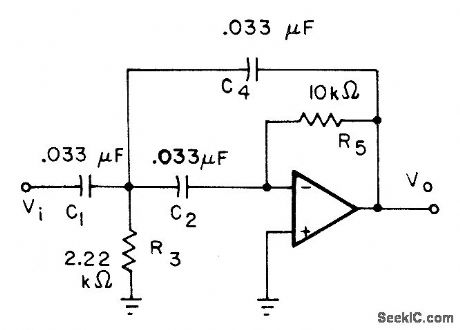
500_Hz_LOW_PASS_UNITY
Published:2009/7/2 20:44:00 Author:May
GAIN-Multiplefeedback filter using 741 or equivalent opamp has unity gain in passband below 500-Hz cutoff.Resistors can be 5% tolerance.-H. M, Berlin, Design of Active Filters, with Experiments, Howard W. Sams, Indianapolis, IN,1977,p 99-1O0. (View)
View full Circuit Diagram | Comments | Reading(759)
1_kHz_SIXTH_ORDER_HIGH-PASS
Published:2009/7/2 20:43:00 Author:May
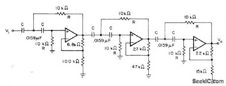
Formed by cascading three different second-order sections,Passband gain is 12.5 dB Opamps can be 741 or equivaient Used when high reiection is needed for signals just below passband,in application where such rejection justifies cost of extra filter sections.-H. M. Berlin, Design of Active Filters,with Experiments, Howard W Sams, Indianapolis, IN 1977, p 122-125. (View)
View full Circuit Diagram | Comments | Reading(962)
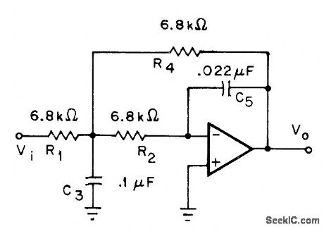
1_kHz_HIGH_PASS_UNlTY
Published:2009/7/2 20:42:00 Author:May
GAlN-Passband gain of 741 or equivalent opamp circuit is set by ratio of C4 to C1 rather than by resistors. Values shown give unity gain for passband above 1-Hz cutoff. Circuit uses multiple feedback.-H. M.Berlin, Design of Active Filters, with Experiments, Howard W. Sams, Indianapolis, IN, 1977, p 100-102. (View)
View full Circuit Diagram | Comments | Reading(580)
OCTAVE_AUDIO_EQUALIZER
Published:2009/7/2 20:42:00 Author:May
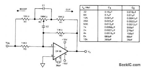
R2 provides up to 12-dB boost or cut at center frequency determined by values of C1 and C2 as given in table.Uses Precision Monolithics OP-08 opamp. Low input bias current of opamp permits scaling resistors up by factor of 10, to reduce values of C1 and C2 at low-frequency end. Same circuit is used for all 10 sections of equalizer, which together draw only 6 mA maximum from supply.- Precision Low Input Current Op Amp, Precision Monolithics, Santa Clara, CA, 1978, OP-08, p 1. (View)
View full Circuit Diagram | Comments | Reading(650)
2-kHz_LOW-PASS
Published:2009/7/2 20:40:00 Author:May
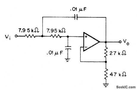
Voltage-contralled voltagesource filter uses equal-value input resistorsand equal-value capacitors, simplifying selection of components Equation for cutoff froquency then simplifies to f=1/6.28RC or 1/(6.28)(7950)(0.01)(10-6) Opamp can be 741.-H.M.Berlin, Design of Active Filters,With Experiments, Howard W.Sams,Indianapolis,IN,1977,p 85-86. (View)
View full Circuit Diagram | Comments | Reading(655)
1_MHz_TRACKING_FILTER
Published:2009/7/2 20:38:00 Author:May

Exar XR-S200 PLLIC is connected to function as frequency filter when phase-locked loop locks on input signal, to produce filtered version of input signal frequency at VCO output. Because circuit can track input over 3:1 range of frequencies around freerunning frequency of VCO, it is known as tracking filter. Optional wideband discriminator output is also provided.- Phase-Locked Loop Data Book, Exar Integrated Systems, Sunnyvale,CA,1978, p 9-16. (View)
View full Circuit Diagram | Comments | Reading(795)
LOW_PASS_AF
Published:2009/7/2 20:36:00 Author:May
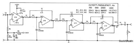
Can be used to attenuate un desired high-frequency audio response in superhet or direct-conversion receivers having inadequate IF selectivity, to improve CW or SSB reception. Resistor values determine cutoff frequency; 700 and 900 Hz are for CW and 2500 Hz for SSB. Insert filter at point having low audio level. Filter has input buffer, three cascaded active low-pass filter stages, and IN/OUT switch.Overall gain is unity. U1 is Fairchild μA4136, Raytheon RC4136, or equivalent quad opamp.Overall response is 1.5 dB down at cutoff frequency, about 36 dB down at twice cutoff, and about 60 dB down at three times cutoff. R7 and R8 provide pseudoground of half supply voltage, to eliminate need for negative supply. Will operate with supply from 6 to 36 V, drawing about 7 mA.-T, Berg, Active Low-Pass Filters for CW or SSB, QST, Aug. 1977, p 40-41. (View)
View full Circuit Diagram | Comments | Reading(916)
1_Hz-500_kHz_VOLTAGE_TUNED_BANDPASS
Published:2009/7/2 20:33:00 Author:May
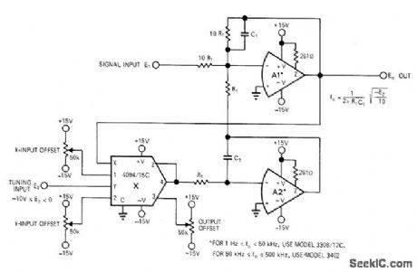
Coupling FET opamps with analog multiplierglves simple two-pole bandpass filter that canbe tuned by external voltage of 0-10 VDC to glve center frequency anywhere in range fromlHzto 500 kHz With components shown,Articleglves design equations,-T,Gate,Voltage Tune Your Bandpass Filters with Multipliers, EDN Magazine,March 1,1971,p 45-47. (View)
View full Circuit Diagram | Comments | Reading(549)
LOW_POWER_SCHMITT
Published:2009/7/2 20:32:00 Author:May

Uses two NAND gates from SN74L00 NAND package and one NOR gate (used as inverter) from CD4001AE CMOS package to make low-power Schmitt trigger. NAND gates are connected to form RS flip-flop. Q goes high when input voltage is greater than 2.1 V, and other output does not go low until input voltage is less than 1.2 V.Both polarities of output signal are available.-R. Cox, CMOS and LPTTL Gates Make LowPower Schmitt Trigger, EDN Magazine, Oct. 1, 1972,p48. (View)
View full Circuit Diagram | Comments | Reading(1782)
1_kHz_STATE_VARIABLE
Published:2009/7/2 20:31:00 Author:May
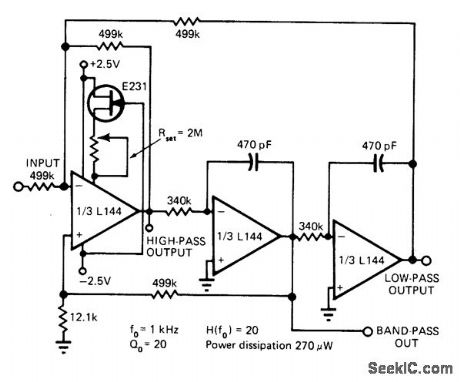
Low-power filter uses three opamps to provide simultaneous high-, low-, and bandpass outputs. Article presents complete design procedure for keeping current drain at minimum while providing desired gain-bandwidth product of 240 kHz.-L.Schaeffer, Op-Amp Active Filters-Simple to Design Once You Know the Game, EDN Magazine, April 20, 1976, p 79-84. (View)
View full Circuit Diagram | Comments | Reading(481)
EXCLUSIVE_OR_LOGIC_FOR_MUTING
Published:2009/7/2 20:28:00 Author:May
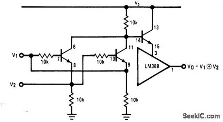
Connection shown for National LM389 combination ofthree transistors with opamp gives standard EXCLUSIVE-OR circuit for controlling muting transistor in audio system,Shorting pin 12 ofopamp to ground gives EXCLUSIVE-NORlogic.- Audio Handbook, National Semicondqctor,Santa Clara,CA,1977,p4-33-4-37 (View)
View full Circuit Diagram | Comments | Reading(590)
ECL_INTERFACE_FOR_VMOS
Published:2009/7/2 20:22:00 Author:May
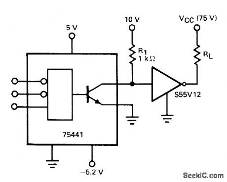
S55V12 VMOS (identical to S55V01 except for higher breakdown/saturation voltage) is used to buffer ECL-compatible SN75441 peripheral driver. Combination is capable of handling up to 90 V at 2 A.SN75441 has open-collector output, so inter-face with VMOS requires only pull-up resistor R1.-L. Shaeffer, VMOS Peripheral Drivers Solve High Power Load Interface Problems, Computer Design, Dec. 1977, p 90, 94, and 96-98. (View)
View full Circuit Diagram | Comments | Reading(1089)
LEVEL_AND_POLARITY_SHIFTER
Published:2009/7/2 20:09:00 Author:May
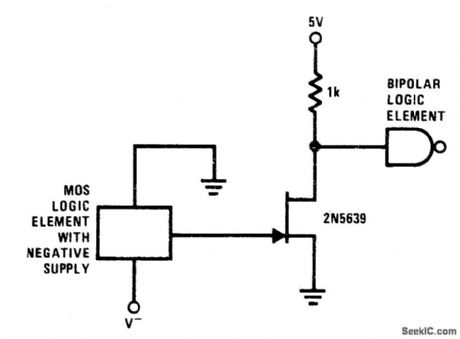
Simple FETcircuit provides for level shifting from MOS logic element having negative supply to TTL orother bipolar logic level operating from positivesupply and ground. Transistor has fast switching time.- FET Databook, National Semiconductor, Santa Clara, CA, 1977, p 6-26-6-36. (View)
View full Circuit Diagram | Comments | Reading(483)
| Pages:287/471 At 20281282283284285286287288289290291292293294295296297298299300Under 20 |
Circuit Categories
power supply circuit
Amplifier Circuit
Basic Circuit
LED and Light Circuit
Sensor Circuit
Signal Processing
Electrical Equipment Circuit
Control Circuit
Remote Control Circuit
A/D-D/A Converter Circuit
Audio Circuit
Measuring and Test Circuit
Communication Circuit
Computer-Related Circuit
555 Circuit
Automotive Circuit
Repairing Circuit